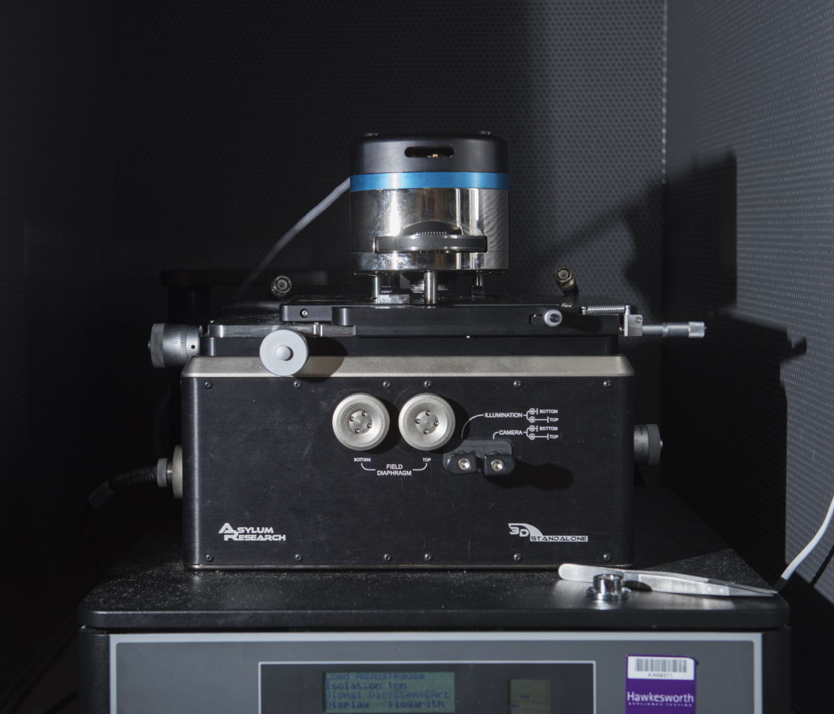
Atomic Force Microscopy (AFM)
Atomic Force Microscope (AFM) can be used to study sufaces of a wide range of sample types down to nanometer lateral and Angstrom vertical resolution. Nanoparticles can be observed, step heights measured or dynamic processes such as crystal growth can be monitored. Images showing topography, force mapping, surface adhesion and electronic properties can be obtained
Applications:
Typical measurements include surface topography and roughness, imaging particles, force/hardness mapping, simultaneous topography and conductivity maps, surface work function variation and nano-lithography.
Typical samples include, but are not limited to, nanoparticles, surface coatings, polymers, biological samples, semiconductors, thin film transistors and substrates.

How does it work?
A sharp tip located on the end of a cantilever is scanned across a surface, which can be in constant contact (contact mode) or with oscillation (tapping mode). The resulting cantilever deflection is measured and converted to the force between the probe and the surface. In advanced techniques tips can be functionalised to introduce specific chemical interactions. Secondary modes can be used in conjunction with topographic imaging, giving information on properties such as conductivity.
Sample handling requirements:
Flat solid samples up to 5 cm in size.
Complementary techniques:
SEM, TEM, STEM, Optical Microscopy
Warwick capability:
Bruker-Nano Multimode V AFM, Bruker-Nano Enviroscope AFM, Bruker-nano Catalyst AFM, Aslyum Research MFP-3D
Contact:
Claire Gerard: / 07385 145064
