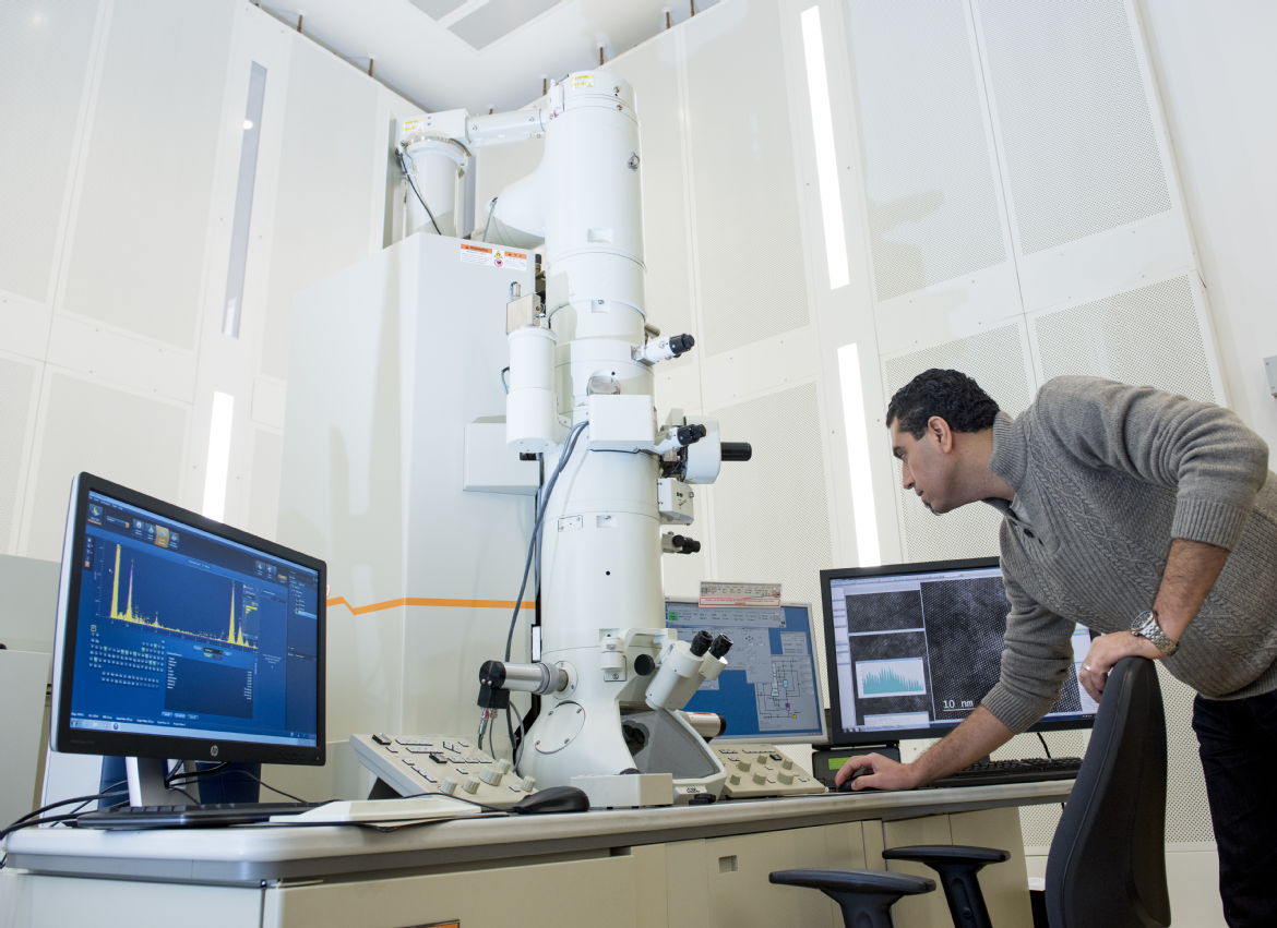
Transmission Electronic Microscopy (TEM)
Transmission Electron Microscopy (TEM) is a microscopy technique whereby a beam of electrons is transmitted through an ultra thin specimen, interacting with the specimen as it passes through.
How does it work?
An image is formed from the interaction of the electrons transmitted through the specimen; the image is magnified and focused onto an imaging device, such as a fluorescent screen, or to be detected by a sensor such as a CCD camera.
TEMs are capable of imaging at a significantly higher resolution than light microscopes, owing to the small wavelength of electrons. This enables the instrument's user to examine fine detail—even as small as a single column of atoms, which is tens of thousands times smaller than the smallest resolvable object in a light microscope.
Applications:
Defect analysis; failure analysis; materials qualification; electron tomography; structural biology; virology; forensics; structural composition; chemical composition; steels; aluminium alloys; ceramics; semiconductor devices.
Sample Handling Requirements:
Samples must be no larger than 3mm diameter, and less than 100nm thick. This means a pre-microscopy ‘sample preparation phase’, using mechanical thinning methods (grinding, polishing, ion-mill, microtome) is required.
Complementary Techniques:
Warwick Capability:
JEOL 2100 TEM-STEM with Gatan Quantum SE EELS-EFTEM, JEOL ARM 200F.

Contact:
Claire Gerard: / 07385 145064
