
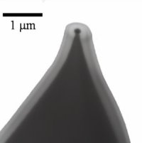
SWNT-based AFM Probes
EFM Probes
SWNT-based Electrical Force Microscopy Probes
The resultant probes can act as higher resolution electrical and topographic probes than are commercially available. For example, using SWNT-AFM tips as probes for electrical force microscopy (EFM) increases EFM spatial resolution allowing similar features to be distinguished with separations as small as 15 nm.1

Figure 1: (a) Topography and (b) ac-EFGM images taken with a nanotube tip; lh=10 nm, Vac=2 V, and Vdc=−2 V. (c) topography and (d) fm-EFGM images taken with a different nanotube tip; lh=5 nm, and Vdc=−4 V. The scale bars are 100 nm. Taken from reference 1.
Nanowire AFM Probes
Nanowire Atomic force microscopy Probes
We have also demonstrated that SWNT-AFM tips act as ideal templates for the formation of metallic nanowire tips for electrical AFM imaging (Figure 2) including conducting-AFM and EFM,2 and present many new opportunities for studying surface phenomena at the nanoscale. For example, nanowire probes show improved longevity over conventional C-AFM probes (thin film of metal coating a Si or Si3N4 tip) as the entire probe is now conducting. Thus tip wear on rough surfaces does not cause a deterioration in the C-AFM signal.

Figure 2: left, FE-SEM image of several SWNTs on a metal coated tip; top center, TEM image of a section of AuPd nanowire; right, TEM image of an Au nanowire tip; bottom center, schematic of nanowire with SWNT core.
SECM-AFM Probes
Scanning Electrochemical-AFM (SECM-AFM) Probes
|
By applying successive insulation layers to gold nanowire AFM probes and cutting across the nanowire using focused ion beam machining, their application can be extended to simultaneous topographical and electrochemical imaging (Figure 3).3 The probes are most suitable for high resolution detection of species diffusing from active sites by operating in the substrate generation – tip collection mode. Figure 4 shows the height image (a) and electrochemical (b) and (c) signal for the reduction of Ru(NH3)63+ at the substrate surface and collection at the probe. |
|
The high electrochemical spatial resolution can be seen through the close similarity between the topographic shape of the electrode and the electrochemical response. The electrochemical data in Figure 4(b) is replotted in Figure 4(c), using a multi-banded colour scheme to emphasise the emergence of pure radial diffusion at larger distances from the electrode, even though the electrode itself is clearly not circular.

Figure 4: Tapping mode AFM height, (a), and electrochemical current, (b) and (c), images of a ~ 2 µm diameter Pt substrate recorded using a nanowire SECM-AFM probe at a scan rate of 0.5 Hz. The images are 20 µm square.
References
- J. V. Macpherson, N. R. Wilson, J. Appl. Phys. 2004, 96, 3565.
- N. R. Wilson, J. V. Macpherson, Nano Letts. 2003, 3, 1365.
- D. P. Burt, N. R. Wilson, J. M. R. Weaver, P. S. Dobson, J. V. Macpherson, Nano Letts. 2005, 5, 639.
Read more about SWNTs:


