
Focussed Ion Beam Lithography (FIB)
Focused Ion Beam, also known as FIB, is a technique used particularly in the semiconductor and materials science fields for site-specific analysis, deposition, and ablation of materials.
How does it work?
An FIB setup is a scientific instrument that resembles a scanning electron microscope (SEM). However, while the SEM uses a focused beam of electrons to image the sample in the chamber, an FIB setup instead uses a focused beam of ions.FIB can also be incorporated in a system with both electron and ion beam columns, allowing the same feature to be investigated using either of the beams. FIB should not be confused with using a beam of focused ions for direct write lithography (such as in proton beam writing), where the material is modified by different mechanisms.
Applications:
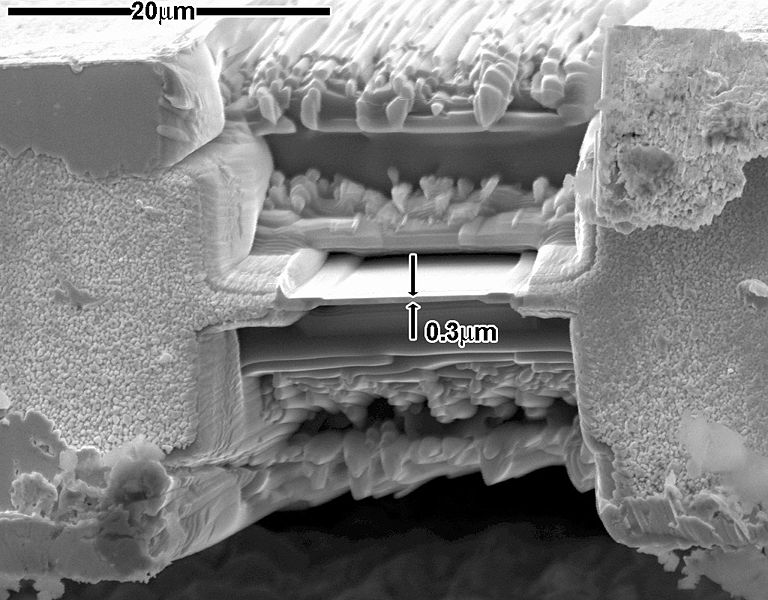
TEM sample preparation; photolithography; defect analysis; etching; polishing and thinning.
Sample Handling Requirements:
Solid <150mm side dimensions.
Complementary Techniques:
Ion Polishing, SEM, TEM, AFM, STM.
Warwick capability:
Contact:
Claire Gerard: / 07385 145064