SWNT-based Electrical Devices
Single Tube Devices
Single tube electrical measurements using field effect transistor devices
In addition to fabricating SWNT-AFM probes, work has been done on the fabrication of electronic devices with individual SWNT as the active component (Figure 1). Initial work has focused on studying conductance through these devices, which can act as single molecule field effect transistors.
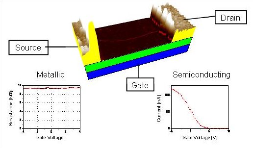
Figure 1: (top) Combined AFM image schematic of an electronic device fabricated by lithographically defining electrodes on top of a single SWNT on an insulating substrate; (bottom) electronic characteristics of SWNT electronic devices.
SWNT Network Devices
Electrical measurements using carbon nanotube networks
The standard thermal cCVD procedure used at Warwick generates a randomly distributed 2D SWNT network on Si/SiO2. Statistically a third of the tubes will be metallic and two thirds semiconducting.
Simple electrical devices can be fabricated from the SWNT networks by patterning metal electrodes on the network. The lithographic procedure is described in Figure 2. If the Si back is contacted, these devices can be used as field effect transistors (FETs). The Si gate electrode is separated from the SWNT network by SiO2, an insulating dielectric. Voltages applied to the gate are capacitatively coupled to the SWNT network and change the network’s electrical properties. If the correct gate voltage is applied, semiconducting SWNTs in the network are electrostatically doped and start to conduct. The current flowing across the network is obviously a function of gate voltage, but also depends on the nature of the network itself.
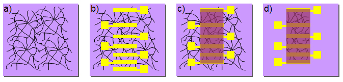
Figure 2: Schematic of the lithographic procedure used for fabricating SWNT network FETs. a) SWNT network grown onto Si/SiO2 by cCVD; b) metal contacts; c) protection with photoresist; d) O2 plasma ashing.
For high density networks, there will be a continuous conducting pathway through the metallic SWNTs. The FET response of such a network is that of a semiconductor overlapped to a constant metallic background. In Figure 3a, notice the non-zero minimum current flowing through the device. Even when the semiconducting SWNTs are negatively doped and switched off, current still flows through the metallic SWNTs. If the density is below the metallic percolation threshold, the response of the network is that of a semiconductor, with the current reaching zero when the semiconducting SWNTs are switched off (Figure 3b).
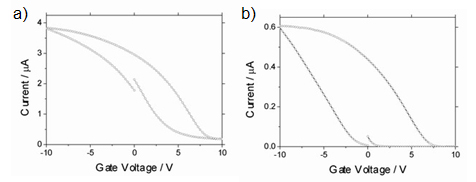
Figure 3: Current as a function of gate voltage for SWNT-network devices constructed from SWNT networks of a) high density; b) low density.
References
- N. R. Wilson, PhD Thesis: Electronic Transport in Single-Walled Carbon Nanotubes and their Application as Scanning Probe Microscopy Tips 2004.
- J. P. Edgeworth, N. R. Wilson and J. V. Macpherson, Small 2007, 3(5), 860-870.
Read more about SWNTs: