Microscopy Group
FULLY FUNDED PHD PROJECTS AVAILABLE!
We are currently recruiting for two fully funded PhD projects for a 2026 start.
Project: Low-dose 4D-STEM electron ptychography for biological dynamic imaging.
Details and Contact: See the project hereLink opens in a new window and contact Prof Peng WangLink opens in a new window to discuss.
Project: Magnetoelectric coupling in 2D materials.
Details and Contact: See the project hereLink opens in a new window and contact Dr Alex RobertsonLink opens in a new window to discuss.
Microscopy Group Research Nuggets
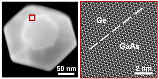
Flux-induced diameter control in GaAs nanowires
Controlling the diameter of self-catalyzed III–V nanowires is important for tailoring their performance in optoelectronic applications. Here, we investigate the impact of abrupt or gradual increase of the V/III flux ratio on the GaAs nanowire diameter.
Capturing defects in diamond caused by neutron irradiation
Understanding radiation-induced damage in diamond is crucial for enabling its practical applications and advancing materials science. We report the atomic-level characterization of high-energy neutron induced diamond defects by atomic resolution TEM and EELS.
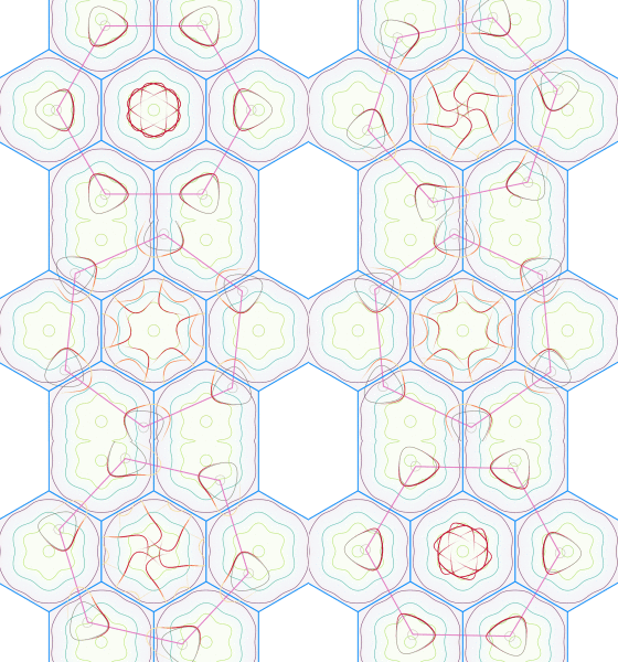
Pyramidal charged domain walls in ferroelectrics
Domain structures play a crucial role in the electric, mechanical, and other properties of ferroelectric materials. In this study, we use high resolution imaging to uncover the physical origins of the enigmatic zigzag domain structure in the prototypical multiferroic material BiFeO3. Using phase-field simulations within the Landau-Ginzburg-Devonshire framework, we demonstrate that spatially-homogeneous defect charges result in domain structures that closely resemble those observed experimentally.
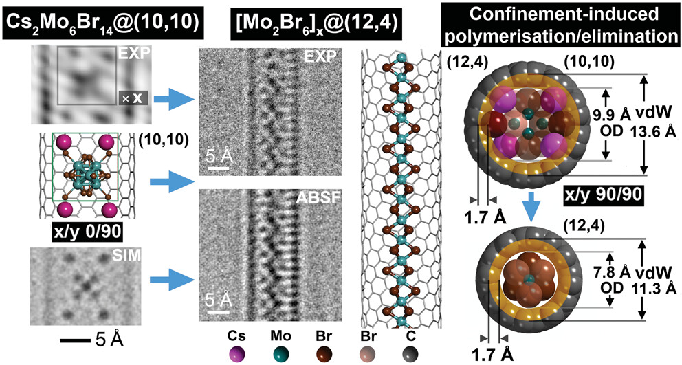
Different packing schemes for Halides in Variable Diameter Carbon Nanotubes
We explore the subtle relationship between the SWCNT internal diameter and Cs2Mo6Br14 cluster packing and find a hierarchical relationship between the nature of the cluster packing and a progressive tendency toward formation of one-dimensional (1D) structures as the SWCNT diameter narrows.
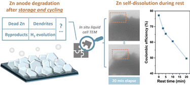
Identifying the role of Zn self-dissolution during anode corrosion in Zn-ion batteries
We use operando electron microscopy imaging to identify self-dissolution of metal zinc under Zn-ion battery aging conditions, which leads to the local pH changes that culminate in the formation of corrosion products.
Conduction band replicas in a 2D moiré semiconductor heterobilayer
Stacking monolayers with a twisted angle gives rise to moiré interference patterns, and can lead to new topological electronic properties emerging. We use ARPES to probe the conduction band of these materials, accessing these edges by applying an electrostatic gating potential across the stacked layers.
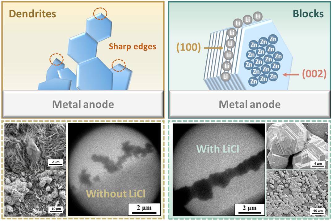
Electrostatic shielding for dendrite suppression in aqueous zinc batteries
Electrolyte engineering is one of the best ways to improve rechargeable battery performance. The aqueous zinc battery is a potentially safe and cheap battery technology for grid-scale storage, yet suffers from poor performance due to dendrite growth. We identify a mechanism for preventing dendrite growth by changing the electrolyte. Click the image to find out more.
ARPES signatures of few-layer twistronic graphenes
Unusual and exotic condensed matter properties emerge when we twist two layers of stacked graphene to be at a shallow angle to each other. We use ARPES to directly probe these electronic structural changes in such "twistronic" devices.
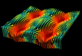
Ferroelectric incommensurate spin crystals
Ferroics can form complex topological spin structures when subjected to particular physical boundaries. A domain structure in a PbTiO3 layer between SrRuO3 electrodes has been discovered with two orthogonal periodic modulations that form an incommensurate polar crystal, and provides a ferroelectric analogue to recently discovered incommensurate spin crystals in ferromagnetic materials. Click the image to find out more.
Interlayer Umklapp hybridisation of bands in 2D heterostructures
Interlayer effects within 2D heterostructures can be studied using spatially-resolved angle-resolved photoemission spectroscopy (microARPES). We show how twist-controlled Umklapp scattering of hybridised electronic states can be used to engineer discrete positions of strong coupling between two 2D materials. Click the image to find out more.
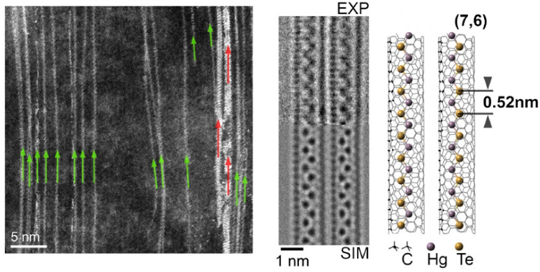
Insights into the Influence of Filling Carbon Nanotubes with Atomic Nanowires
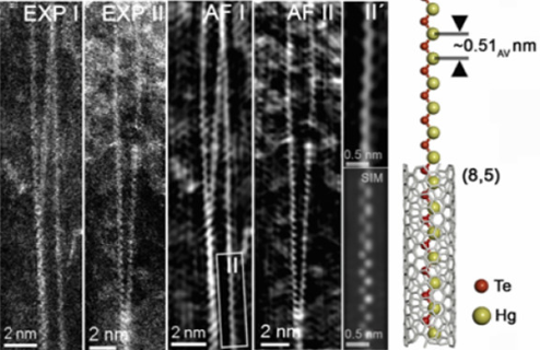
We report comprehensive spectroscopic studies of how infiltrated HgTe nanowires (NWs) alter the optical properties of small-diameter (< 1 nm) single-walled carbon nanotubes (SWCNTs) in different environments.
The Electron–Phonon Interaction for HgTe Nanowires inside Carbon Nanotubes
Atomically thin nanowires (NWs) can be synthesized inside single-walled carbon nanotubes (SWCNTs) and feature unique crystal structures. Here we show that HgTe nanowires formed inside small-diameter (<1 nm) SWCNTs can advantageously alter the optical and electronic properties of the SWCNTs.
Current-Density-Dependent Electroplating in Ca Electrolytes
Calcium-ion rechargeable batteries are promising emerging candidates for beyond lithium-ion, in part due to the better stability of calcium metal. To exploit this advantage we need to better understand how new calcium electrolytes perform, and particularly the conditions under which dangerous metal dendrites may form. We use operando electrochemical TEM, effectively a micro-battery operated inside the microscope, to image dendrite formation in real-time. Click the video to find out more.
Direct observation and catalytic role of mediator atom in 2D materials
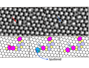
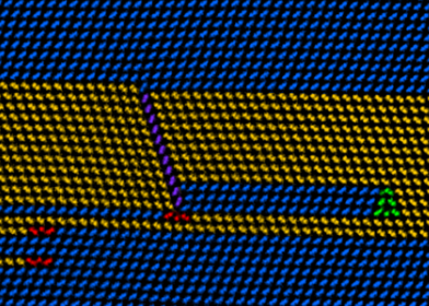
Atomic defects govern material behaviour, most clearly seen with the case of dislocation migration and plasticity. It is understood that defect changes occur via sequential atomic bond rotations; however, modelling tells us the energy barrier for these are high. By combining monochromated aberration corrected TEM imaging of graphene - resolving individual carbon atoms - with TBMD and DFT modelling, we reveal the role of surface adatoms in mediating lower energy defect migration mechanisms. Click the image to find out more.
AI-enabled Cryogenic Electron Ptychography For Bio-macromolecule Imaging
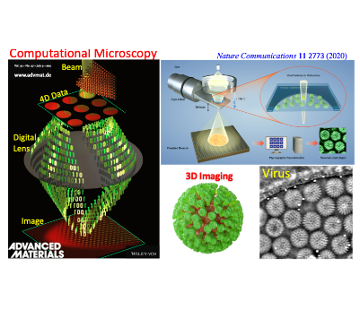
Nobel Prize winning technique, cryogenic electron microscopy (cryo-EM) is a powerful method for visualizing a wide range of biological macromolecules in three dimensions at near-atomic resolution, which can provide direct insights into function and mechanism. Here, we are developing a completely new computational microscopy so called cryogenic electron ptychography, further enhanced by artificial intelligence (AI) and machine learning techniques to recover high fidelity amplitude and phase contrast images of biological macromolecules with state-of-the-art ultrafast detectors at low dose. Click the image to find out more.
Development of in situ Multi-channel 5D STEM Imaging for Functional Materials
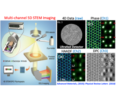
Unlike conventional imaging modes, we are developing novel computational diffractive imaging techniques (ptychography, 4D STEM) at a cryogenic temperature together with “big data” processing methods and exploiting opportunities by accelerating its application in functional materials ranging from battery to quantum materials. Furthermore, we are looking at dynamic behaviours of materials in situ and study how they respond to a changing external stimulus (such as electric, magnetic field, temperature and light) at timescales required. Click the image to find out more.
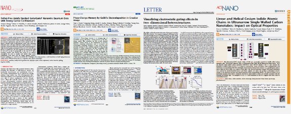
Visualizing electrostatic gating effects in 2D heterostructures
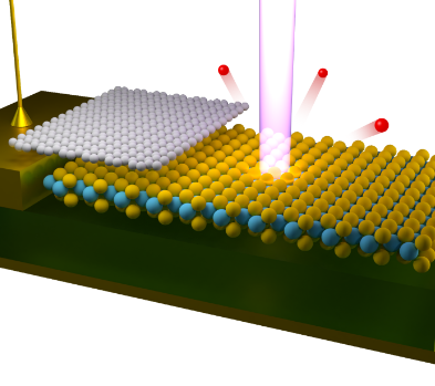
The ability to directly monitor the states of electrons in modern field-effect devices could transform our understanding of the physics and function of a device. We show that micrometre-scale, angle-resolved photoemission spectroscopy (microARPES) applied to two-dimensional van der Waals heterostructures affords this ability, visualizing field-dependent band structure with in-operando measurements. Both optical spectroscopy and microARPES can be carried out on a single device, allowing definitive studies of the relationship between gate-controlled electronic and optical properties. Click the image to find out more.
Revealing Defect Dynamics in III-V Nanowires
For functional applications in next generation technology, semiconductor nanowires should be free of defects that can be detrimental to device performance. Defects in self-catalysed nanowires, produced with sub-optimal growth conditions, have been analysed to identify defect types. In-situ microscopy has been utilised to probe defect dynamics and helps us to understand how to improve nanowire quality. Click the image to find out more.
D-LACBED: Digital Large Angle Convergent Beam Electron Diffraction
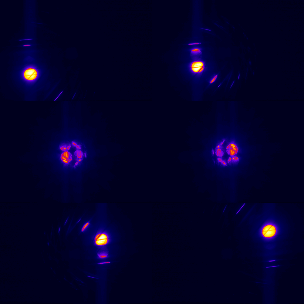
By combining lots of individual CBED patterns acquired using computer control of beam tilt, LACBED patterns can be reconstructed. The LACBED patterns provide a wealth of information about sample symmetry and can even be used to solve crystal structure. Click the image to find out more.


