
Light Emitting Diode under TEM
After examining the LED in the Scanning Electron Microscope, we would examine using the Transmission Electron Microscope. Before we could examine it however, the LED had to be prepared so that it would work under the TEM. This required sanding and milling it down to less than a few microns thick.
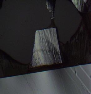
LED, less than a few microns thick.
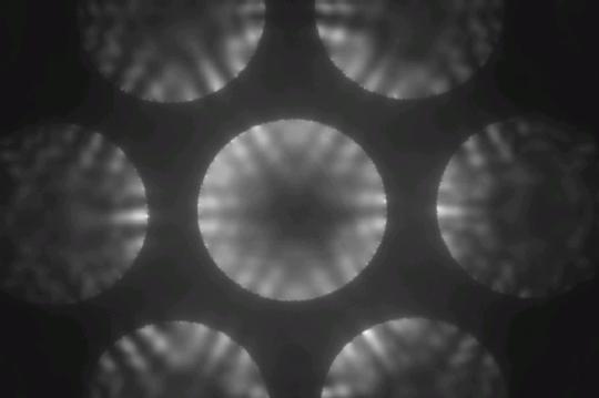
One can see how thin the sample is around the edges, where interference patterns appear, caused from the light bouncing off the back of the sample and interfering with the light bounding of the surface of the sample. This tells us that the sample is as thick as the wavelength of light, or several multiples of the wavelength at that point. The sample has to be this thin, for the TEM to work.
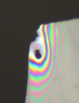
Interference patterns on the LED
We then placed the LED into the TEM and examined it at a much higher magnification than previously possible.
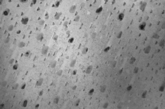
The first image we took under the TEM mainly showed us the dirt that had got onto the sample.
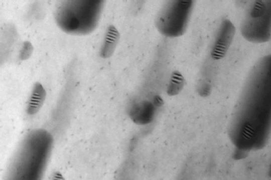
When we zoomed in further we saw Moiré fringes appear in the dirt.
We were able to obtain an electron diffraction pattern which would help us discover what the spacing between the planes of atoms were.