Chip under the TEM
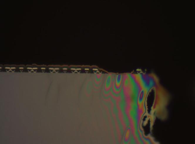
We prepared the chip for placing in the TEM the same way as the LED, and a picture of the sample we placed in is shown below, taken with an optical microscope.
We would be examining the region along the top of the sample, to see the transistors.
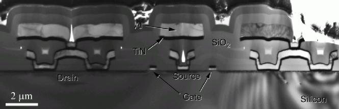
Below is the first picture we took using the TEM of the transistors on the chip. This was a very low magnefication, only 1200x, and showed the component parts before we zoomed in even further. One can see the different drains and source, along with the gates used to control the current. Different layers can also be seen, where different layers of oxide havae been grown on the silicon chip.
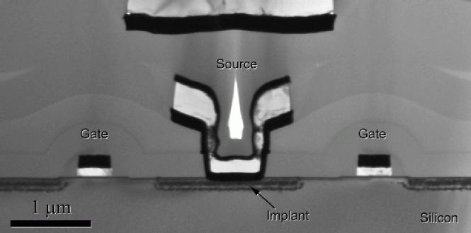
The picture below is taken zoomed in 4000 times. This shows the source for the transistor, with a gate either side.
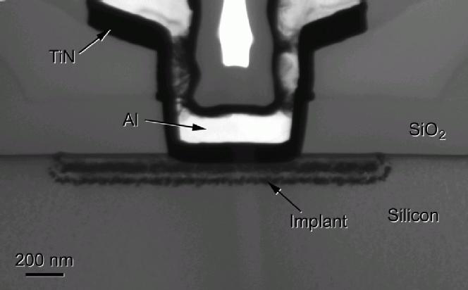
The picture below is taken, zoomed in 10,000 times. It shows the source on top of the implant, in a silicon layer, surrounded by silicon dioxide.
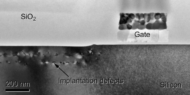
This picture shows one of the gates, and defects in the silicon near it. These came from the manufacturing process.
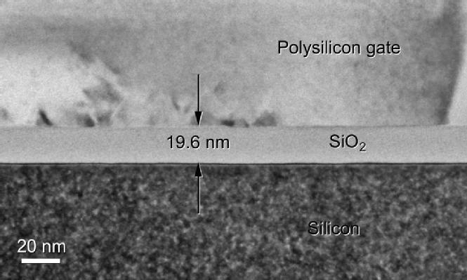
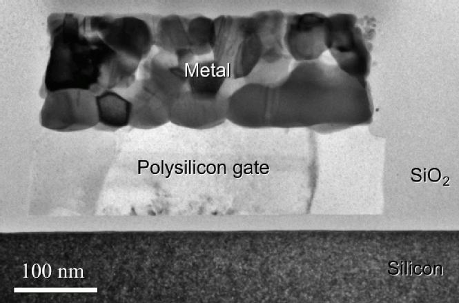
The picture below shows the gate in greater detail. One can see there is a gap between the Polysilicon gate and the silicon base, which acts as a parallel plate capacitor, which can be used to the manipulate the surrounding electric field. There is a metal cover on top to improve the conductivity of the gate.
The final picture we took of the gate was zoomed in 100,000 times. Here we can measure the gap between the gate and silicon to be 19.6nm or around 200 atoms thick. Generally, the smaller the gap, the better the gate can work, but this gate works at a too high voltage, and is also around 10 years behind current standards.