
Polymer Imaging
Polymers have a wide range of applications, with conjugated polymers being used in flexible electronic applications such as organic photovoltaics, transistors, light emitting diodes and sensors. In order to optimise these materials for use in devices, we need to fully understand the characteristics of the polymer microstructure. We have developed a technique for depositing and subsequent high resolution scanning of polymers.
The Technique
The polymer imaging technique uses a combination of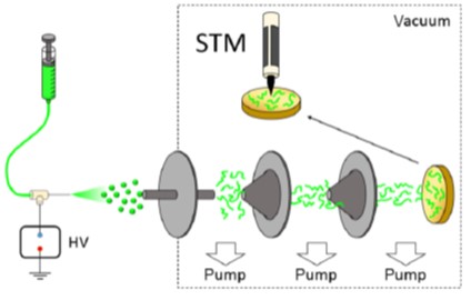 vacuum electrospray deposition (ESD) and low temperature scanning tunnelling microscopy (STM) to achieve high resolution images under ultra-high vacuum.
Schematic representation of the polymer imaging technique is shown to the right.1
Our ESD system is from Molecularspray Ltd with four differential pumping stages. The ultra-high vacuum STM is a SPECS Aarhus 150 instrument with cooling to -143 oC.
What can it show?
The technique can image individual molecular species with sub-nanometer resolution. It can be used to identify monomer units and side chains to provide a precise sequence of polymer structure. It enables the user to understand the nature, number and position of defects on a polymer backbone. Example images are provided below.
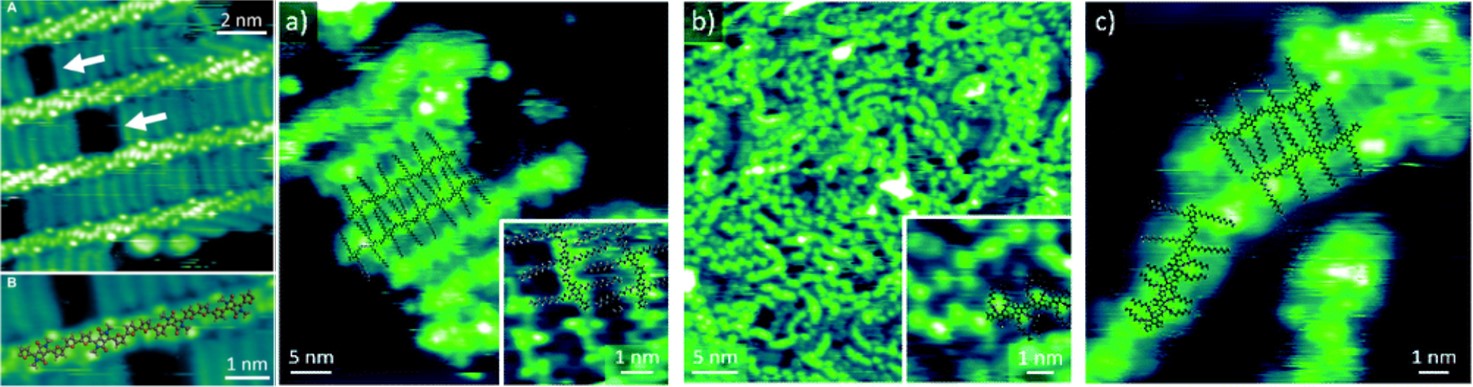
Left to right: Top and bottom, images of C14DPPF-F polymers on Au(111);1 a) PTBnDT homopolymers;2 b) PTBT homopolymers;2 c) PTBnDT-stat-PTBT copolymer.2
Contact Us:
Professor Giovanni Costantini
Email: G.Costantini (at) warwick.ac.uk
Tel: +44-(0)-24-765-24934
References
1 D.A.Warr et al. Sci. Adv. 2018, 4, eaas9543
2 S.S.Lawton et al. Sustainable Energy Fuels, 2020, 4, 2026–2034