
RTP Capabilities
Imaging Surfaces
The main techniques available for imaging surfaces include SEM, AFM and optical microscopy. For more information on these techniques click on the images below.
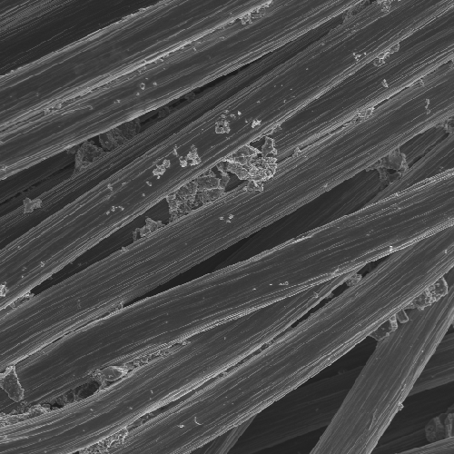
SEM image of Waterproofed Fabric
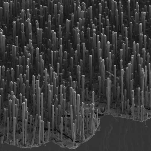
SEM image of GaAs Nanowires
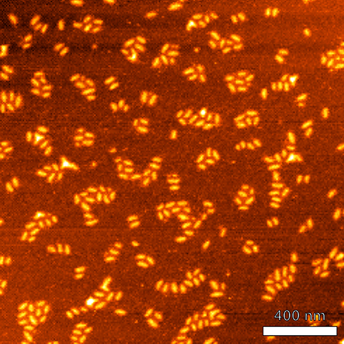
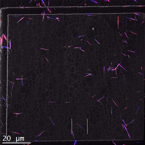
AFM image of Polymer Molecules

Imaging Structure
Information about the structure of a material can be found using combination of TEM, STEM and diffractive imaging. For more information on these techniques, click on the images below.
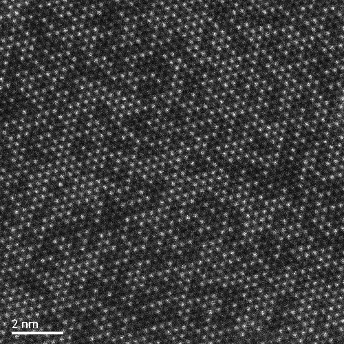
ADF STEM image of Mo0.25W0.75S2
TEM of InAs Quantum Dots within InGaAs Quatum Wells

HDR Diffraction Pattern from a Pc2ScTaO6 Crystal
Spectroscopy
Elemental analysis can be performed on many of our microscopes. Optical spectroscopy is also available using a cathodoluminescence system. For more information on these techniques, click on the images below.
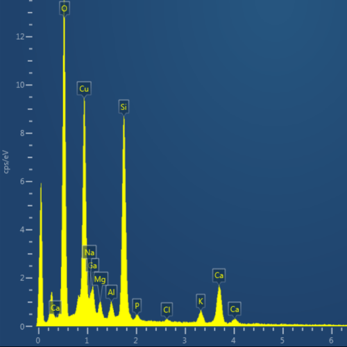
EDX spectrum of Stained Glass specimen
TEM of InAs Quantum Dots within InGaAs Quatum Wells
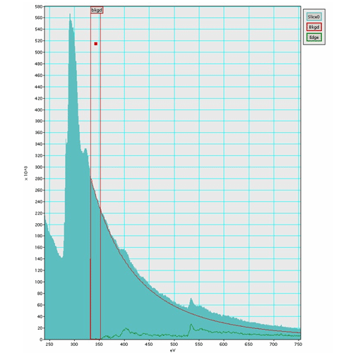
CL map of GaAs nanowires
Cross Sectioning and Sample Preparation
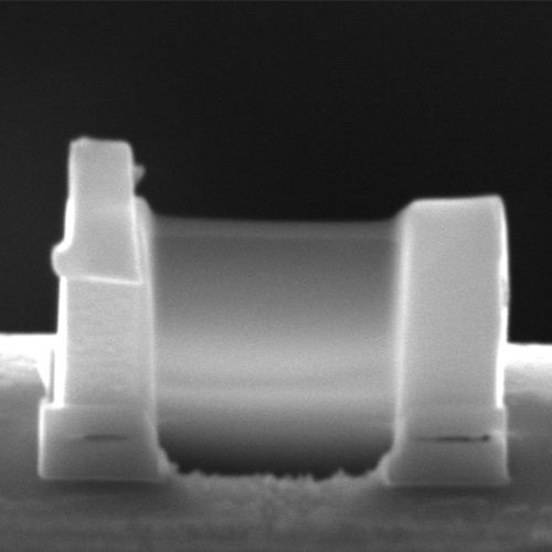
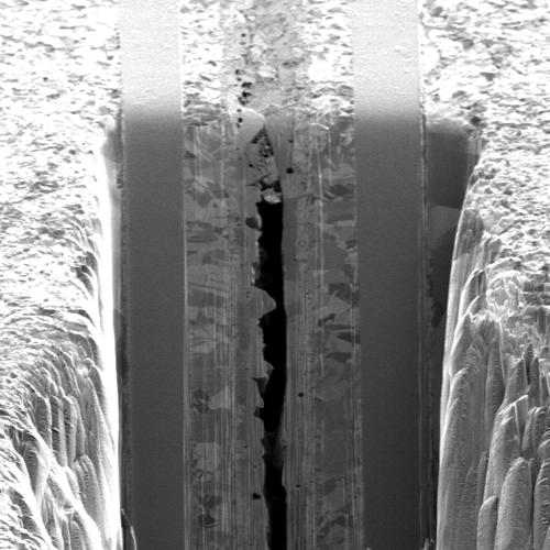
Cross-sectioning and TEM sample preparation is frequently performed using our FIB-SEM, providing sub-micron accuracy when location is important. We also have a well equipped preparation lab, with mechanical and ion polishing machines, sputter coaters and a plasma cleaner. For more information on these techniques, click on the images below.
TEM sample prepared using the FIB lift-out technique
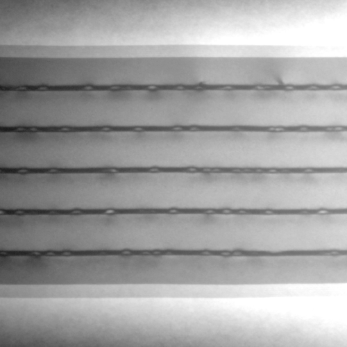
FIB cross-sectional trench revealing a defect in copper alloy bonds
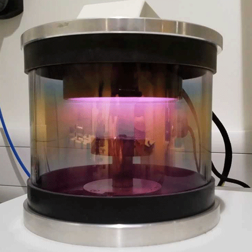
Gold Sputter Coating of an SEM sample