
Project Objectives
Cost: There are continuing demands on reducing the costs of applying power electronics, in some cases the power semiconductors components are commodity items where the economies of scale apply. In many other applications the devices are almost bespoke, as the cost benefits are derived at the systems level.
Power density: In shrinking system size and increasing the power being switched, there is a major issue around power density. Advances are needed in the state-of-art of compact and reliable power semiconductor devices, passive components, electrical machines and converters, alongside reliable packaging and thermal management technologies.
Increased efficiency: In the conversion of electrical energy, inevitably some of the energy will be converted into heat; which must be rejected by the system. Energy lost as heat must be paid for and so efficiency is a key attribute. Also in mobile systems the cooling system is very significant in determining the size and weight of the system, as well as the required battery capacity/recharge time.
Reliability: Semiconductor technology has developed to the point where for silicon the reliability of the systems is mainly determined by the packaging of the device and not the semiconductor itself. With new materials (SiC, GaN) come new challenges, and there are apparent new mechanisms inherent in these systems that are different to silicon. Manufacturability: Key to innovation is ability to manufacture. New devices and processes will need to be practically manufactured at a commercial scale if they are to exploited.
Functionality: The replacement of classical electromechanical devices with their solid-state counterparts allows systems to have new levels of configurability and flexibility and so are not just replacement parts but system enablers.

Device reliability and physics of device failure - Weibull plot of the generation time of defects as identified by electroluminescence in GaN transistor device; inset shows an electroluminescence image of the device, illustrating its degradation during device operation under the operation conditions chosen.
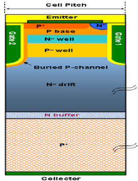
Triple well/dual channel IGBT structure. The triple well helps to reduce the collection of holes during the on-state operation, thus ensuring higher electron injection (for low on-state voltage) while the second gate helps to speed up the collection of holes during the turn-off. The equivalent circuit shows the presence of the second low gain pnp bipolar transistor which inhibits the collection of holes during on-state. This transistor is bypassed with the p-channel depletion mode FET during turn-off.