
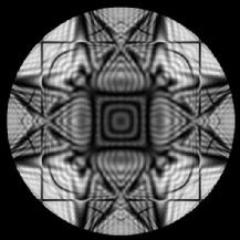
Solving crystal structures with D-LACBED
The information obtained from the CCD cameras on TEMs is quantitative and can be analysed for intensity. As the earlier simulations show, if the crystal structure is known, the experimental pattern can be quantitatively compared to simulated images.
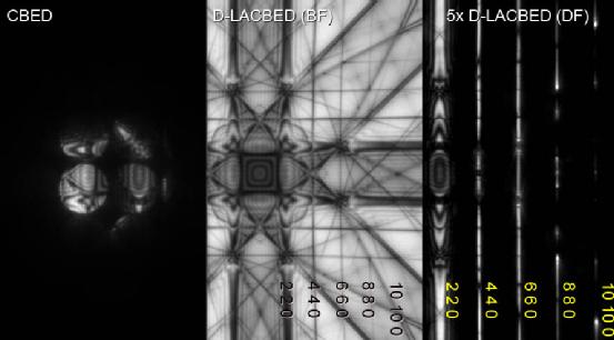
Here is an intensity plot taken from the 000 D-LACBED pattern. The differences between experiment and model arise from two sources: (a) inelastic scattering effects and (b) incorrect values for the electron density in the model.
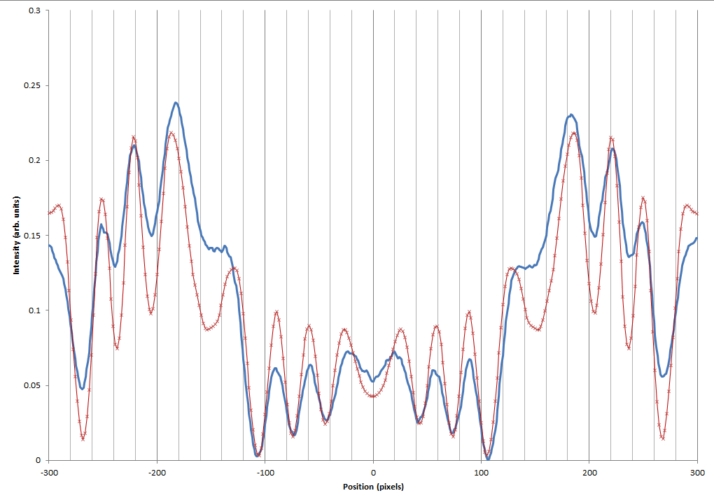
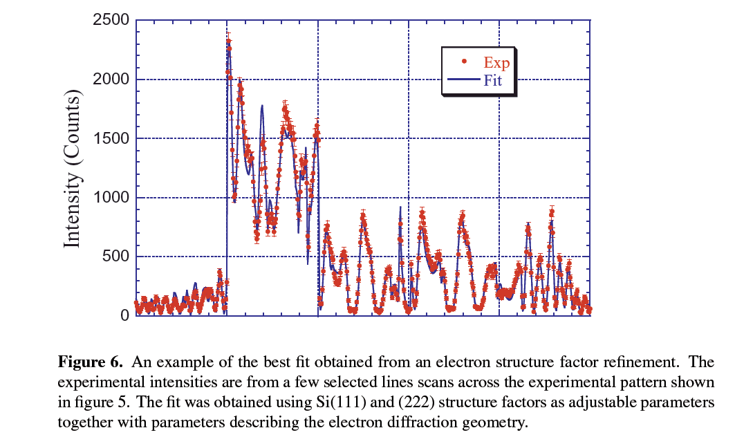
Inelastic scattering can be removed using energy filtering, and by changing the electron density in the crystal it is possible to get a good fit. This has been known for some time; the figure below showing a fit of an energy-filtered CBED pattern is taken from Zuo, Measurements of electron densities in solids: a real-space view of electronic structure and bonding in inorganic crystals, Rep. Prog. Phys. 67 (2004) 2053–2103.
Digital diffraction offers the possibility of being able to perform this process automatically for a large number of diffracted beams. This will give a simple and easy to use route to direct structure solution and refinement using electron diffraction - something which has required a lot of time and effort until now.