A
Shining a light on the future of semiconductors
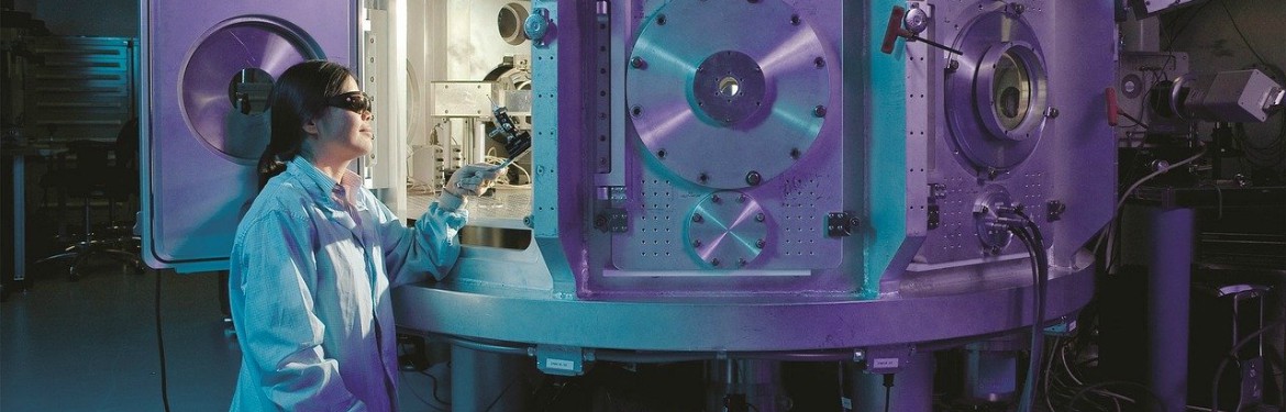
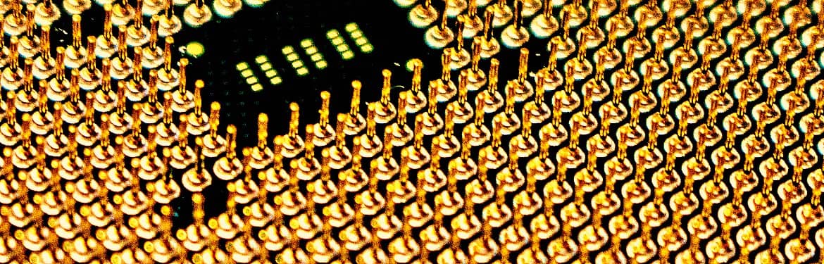
The silicon chip is the basis of all modern electronics. Under strain its crystal lattice distorts and electrons move faster within the structure. When layered with germanium (a rare earth metal), this speed increases further. A team from the Department of Physics researched and built wafers using this ground-breaking technology. Computing and solar power alike have benefited from this step change in electronics.
Mixing silicon and germanium is difficult to achieve. Germanium atoms are spaced 4% further apart than those of silicon. Growing the lattices together created tiny breakages. Small those they were, these were enough to disrupt the structure. The project had to search for a new way to combine the two elements. The alloy needed just enough tension to raise electron speeds within the structure. Any more or any less, and the material would hold back device performance.
The Warwick team developed a multi-stage process to overcome the challenges of mixing silicon and germanium:
Smooth buffer layers to separate the materials (‘virtual substrates’)
A mixture of tensile and compressive strain, depending on the layer
Thin and thick deposits of germanium, grown at different temperatures
AdvanceSis, a spin out company, developed the technology further. The success of this process opened the door to further innovations. For the first time, combining silicon electronics with optical materials (such as those used in LEDs) became a possibility.
The technology created by the Department of Physics has already found many uses. Solar panels generated electricity twice as efficiently by including the alloy material. Carmakers and electronics giants were keen to work with Warwick to gain from this breakthrough. These included companies such as Siemens, Phillips and the Daimler group. With the demand for consumer electronics and solar power growing constantly, this upgrade to the silicon chip will only become more important.