
Research Interests and Projects
Research Interests
My research interests focus on state-of-the-art electron microscopy across a wide range of materials. I have investigated a wide range of materials in collaboration with long-standing co-workers across the UK, Europe and USA. Since my arrival to Warwick I have established myself as the leading UK electron microscopist in novel semiconductor structures, particularly Nanowires and developed an interest in Functional Oxides and Relaxors. Other interests include semiconducting 2D materials, and Quasi-One-Dimensional van der Waals Crystal, ie. semiconductor Nanoribbons less than 10 atoms. Although these examples may seem disparate, they all rely at a fundamental level on the ability to measure the precise location and type of atoms in structures only a few nm in size, which is my speciality. The collaborations are reciprocally very valuable, allowing me to develop new electron microscopy and spectroscopy techniques to determine the structural properties of novel materials and interfaces. This is fundamental information, without which no scientific understanding of materials could be ascertained. Often, structures in this size range have properties that differ massively from the bulk, and these researchers value the characterization and difficulty of precise measurements in nanosystems. There are applications in many fields and I am always seeking to build existing collaborations, make new ones and to find new fields in which to work. Therefore, my research interest may be summarised as:
- Structural characterization of functional materials using high-end electron microscopy.
- Electron Energy Loss Spectroscopy (EELS), in particular plasmon excitations.
- Developing new analysis techniques.
- Semiconductor nanowires
- Piezoelectric, ferroelectric and multiferroic materials: Polarisation, phase transformation, domain switching in ferroelectric thin films.
- 2D Transition metal dichalcogenides.
- Quasi-One-Dimensional van der Waals Crystals.
- Thin films and nanostructures, particularly semiconductors such as III-V-Sb, III-Nitrides, SiC and related materials.
Semiconducting III-V Nanowires
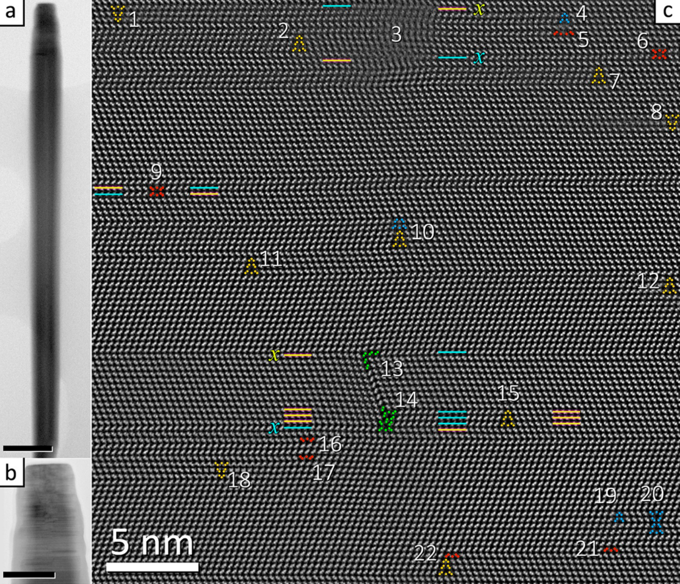
Defects in III-V semiconducting nanowires
(a) BF-STEM image of a Ga-droplet catalyzed NW, with the droplet converted into GaAsP at the end of the growth. Scale bar = 200 nm. (b) BF-STEM image of the top of the NW, showing highly defective material. Scale bar = 100 nm. (c) Atomic resolution ADF STEM image of a defective region.
Nano Lett. 2018, 18, 3081
2D Transition Metal Dichalcogenides
1D interface between 2D semiconductors
(a) Atomically resolved ADF STEM image of an area of the interface between MoSe2 (darker) and WSe2 (brighter).(b) Color plot of intensities at the lattice sites (c) Intensities for the transition metal (Mo, W) sublattice sites only (d) Intensities at the Se sublattice sites only. Scale bar: 1nm.
Nature Mater. 2014 13, 1096
Relaxors
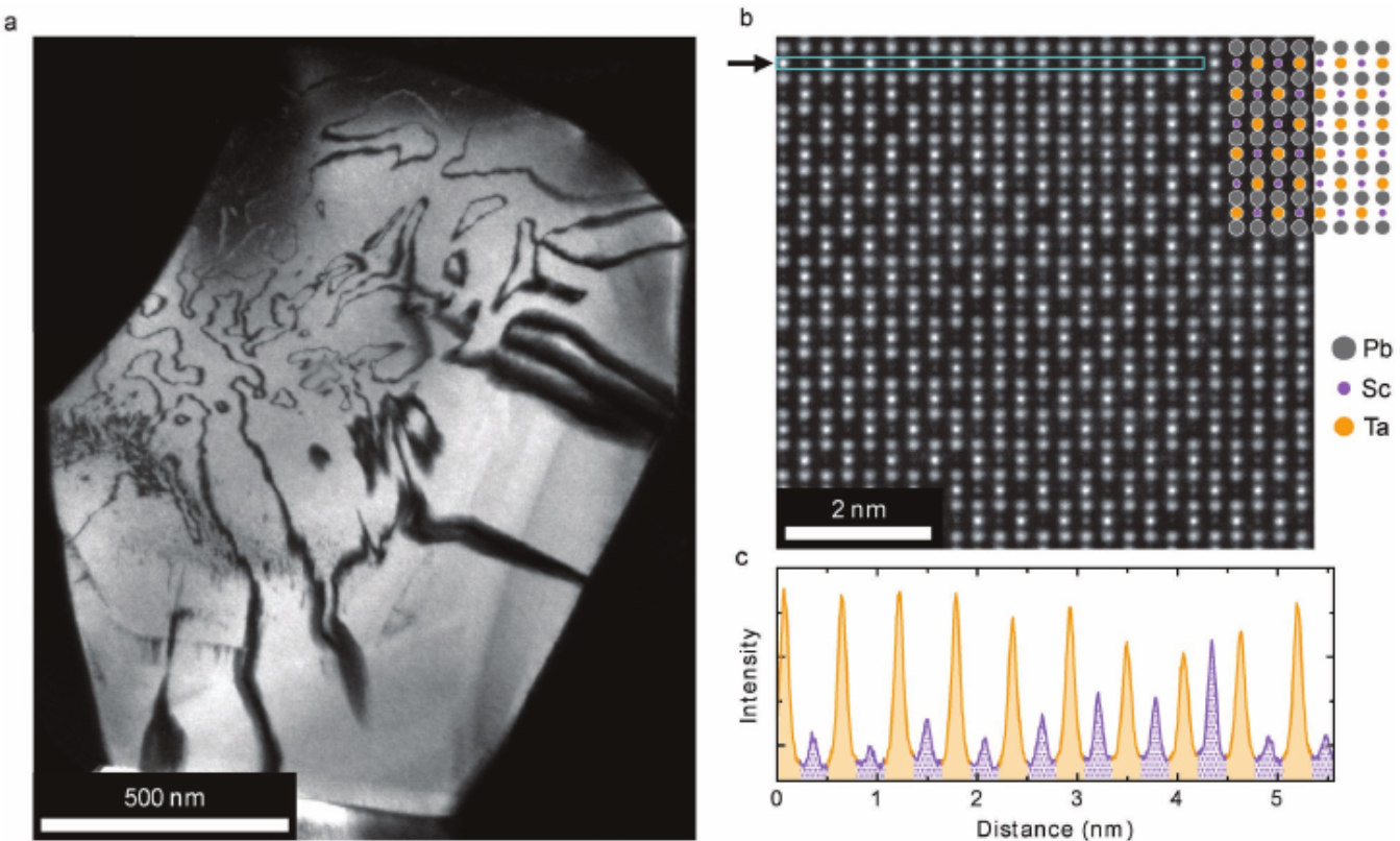
Ordering in Pb2ScTaO6
(a) DF g= 111 image of a single grain of PST. Bright and dark regions show ordered regions and APBs respectively. (b) Atomic-resolution ADF image from (a) with strong ordering clearly evident. (c) An intensity line profile from the region indicated by an arrow in (b). Columns that are expected to contain Sc and Ta are highlighted purple.
Adv. Mater. 2019, 31, 1806498
Ferroelectric oxides
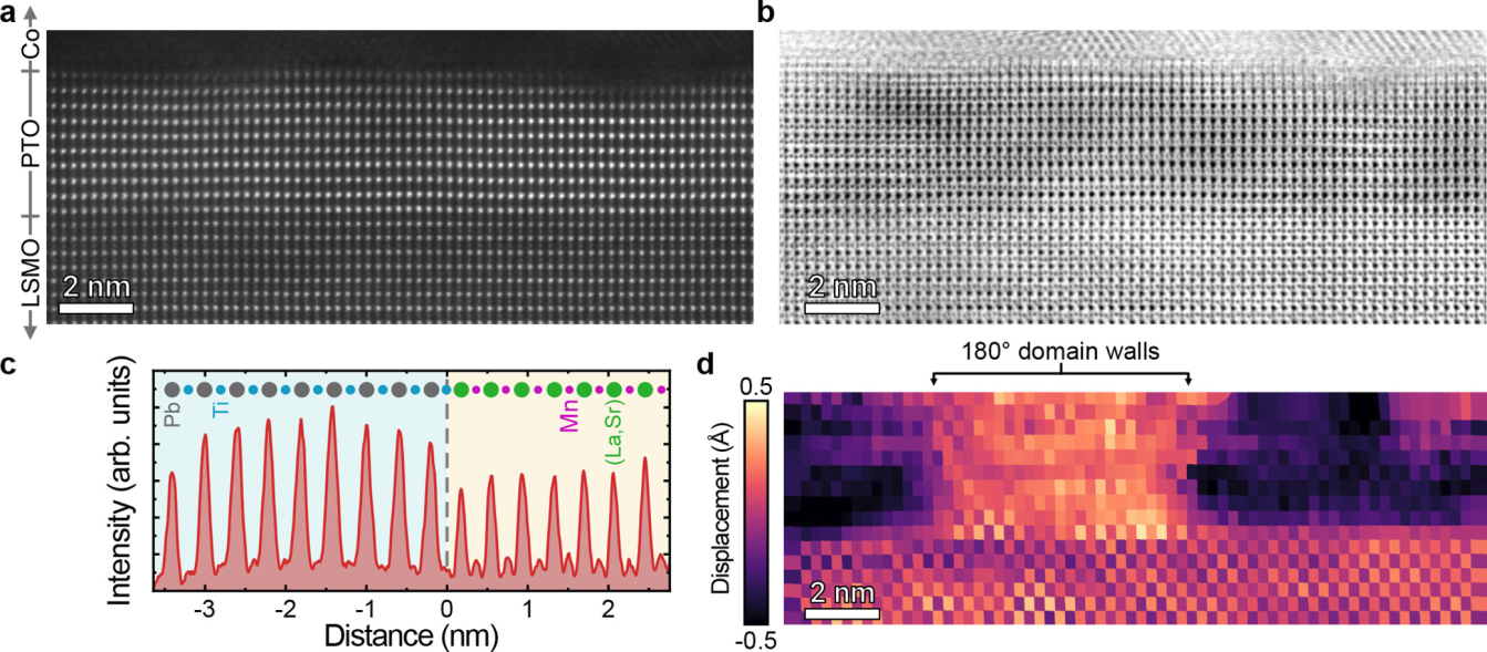
Domain polarization in PbTiO3
(a) ADF and (b) ABF images of the LSMO–PTO–Co FTJ. Contrast in the ADF image gives elemental information, with higher atomic number elements being brighter. (c) Out-of-plane ADF intensity profile where the atomic columns have been identified. (d) Map of the out-of-plane displacements of the O columns with respect to the A lattice.
ACS Appl. Mater. Interfaces 2020, 12, 9, 10657
Complex Functional Oxides
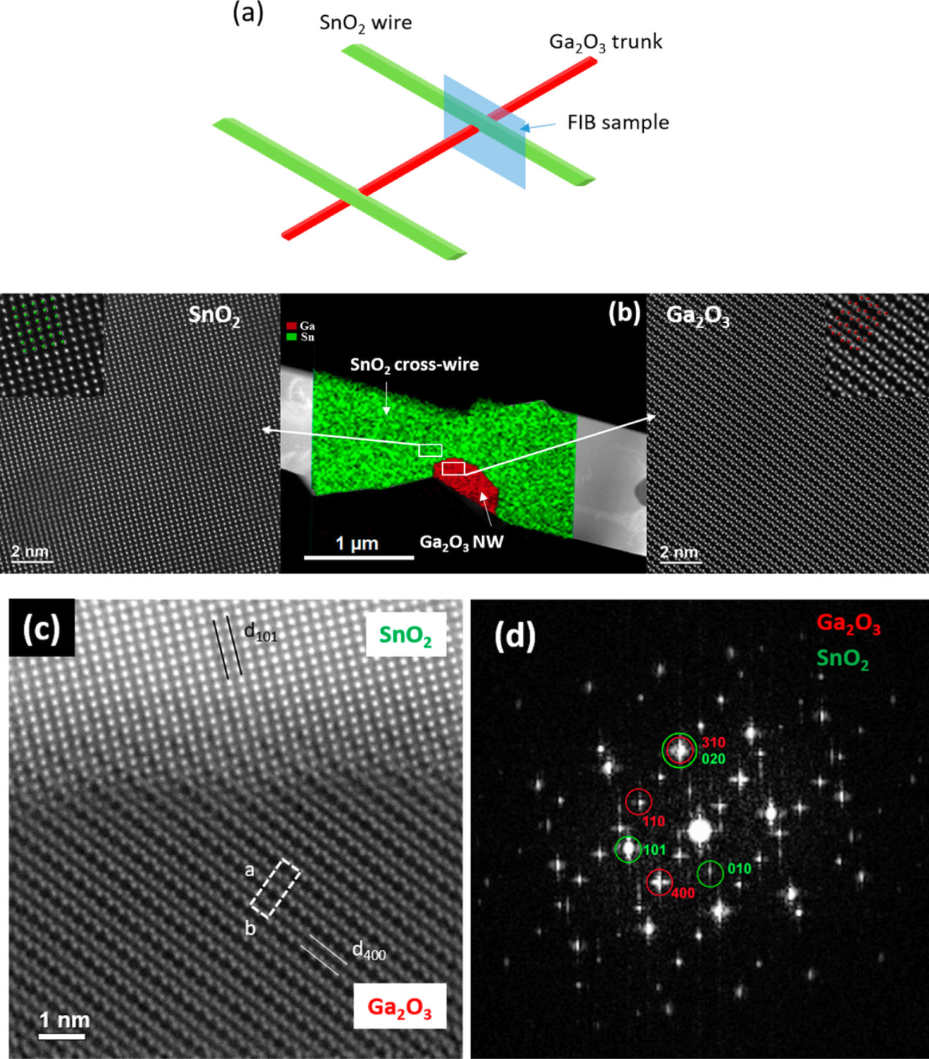
SnO2/Ga2O3 complex nanostructures
(a) Schematic of the junction cross-section. (b) FIB section area of crossing wires (central image) overlapped with EDX compositional information (Ga in red, Sn in green). Left and Right: Atomically resolved STEM of SnO2 central Ga2O3 wires respectively. (c) Atomically resolved ADF image of the heterojunction. (d) FFT of (c) that reveals lattice coincidence between {310} planes in Ga2O3and {020} in SnO2.
Nano Lett. 2017, 17,515
Quasi-One-Dimensional van der Waals Crystal
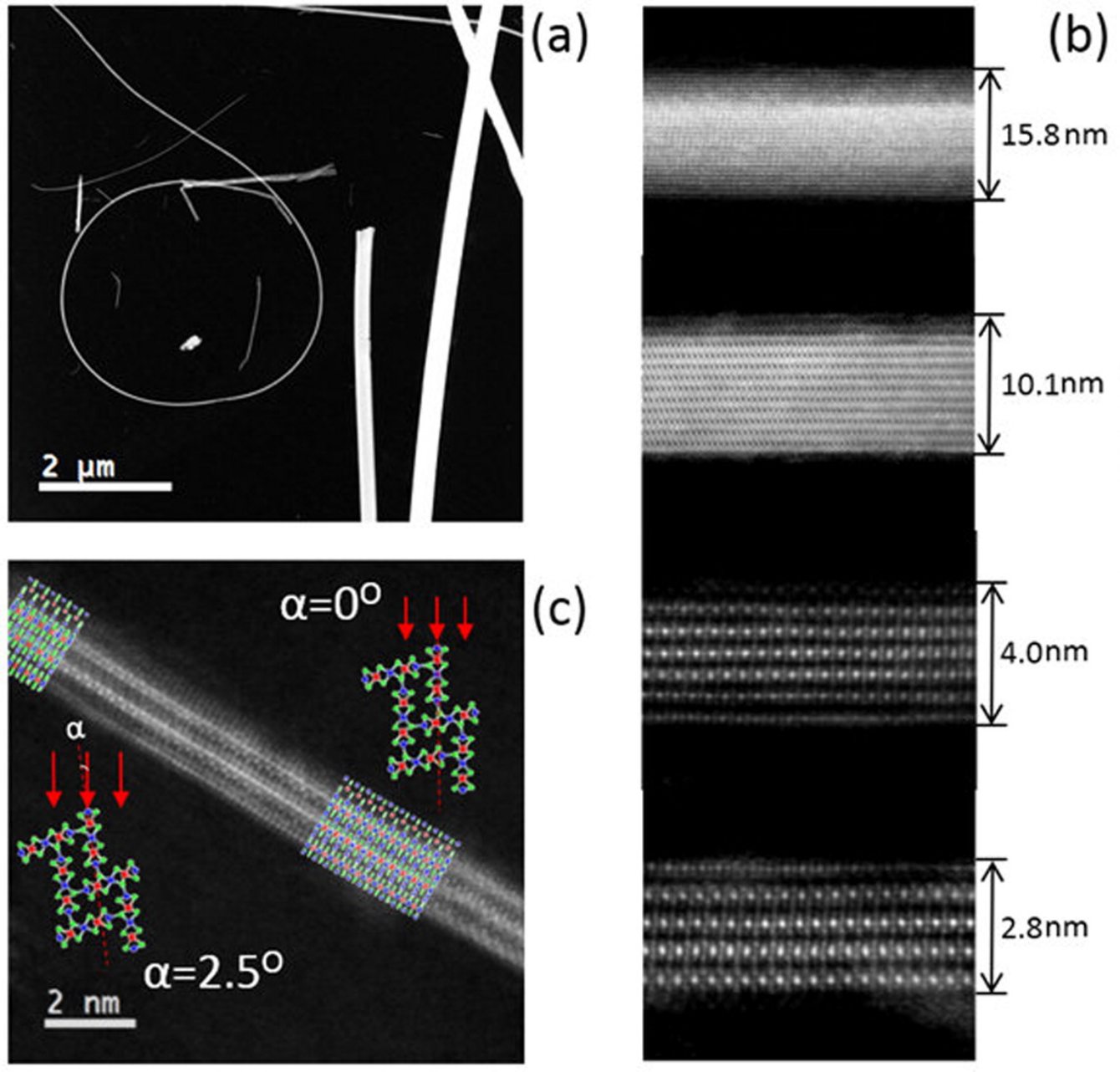
Exfoliated Ta2Pd3S8 nanowires
(a) Low-magnification ADF image of TPdS nanowires. (b) Atomic resolution ADF images of nanorribons with thickness ranging from 15.8 to 2.8 nm. (c) ADF image of a nanowire with 2.1 nm thickness.
Nano Lett. 2016, 16, 6188
Projects
Phosphide-based nanowires for visible and near-infrared miniature photon emitters (EP/W002418/1),Sanchez A.M.April 2022-October 2025 |
New directions in high temperature dielectrics: unlocking performance of doped tungsten bronze oxides through mechanistic understanding (EP/V053701/1)Beanland R, Sanchez AM and Seen MSApril 2021 -April 2024 |
Electric Fields by 4D scanning transmission electron microscopy (EP/V028596/1)Sanchez A.M., Beanland R., Alexe M. and Shah V.A. 2021 - 2024 |
Ferroelectric gating for agile and reconfigurable 2D electronics (EP/T027207/1)Alexe M., Sanchez A.M. and Wilson N.R. July 2020 - December 2023 |
Ferrotoroidic structures: polar flux-closure, vortices and skyrmions (EP/P031544/1)Alexe M. and Sanchez A.M. July 2017 - January 2021 |
GaAsP-GaAs nanowire quantum dots for novel quantum emitters (EP/P000916/1)Sanchez A.M. August 2016 - October 2020 |


Professor Ana Sanchez
Department of Physics,
University of Warwick,
Coventry
CV4 7AL
Office: MAS1.02
Office tel: +44 (0)24 761 51372
Lab tel: + 44 (0)24 765 74476
E-mail: a dot m dot sanchez at warwick dot ac dot uk