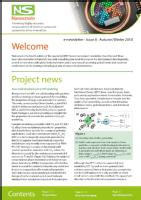
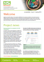
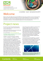
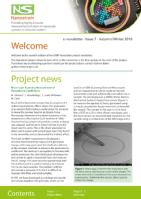
EMRP Nanostrain Project
XMaS is pleased to be involved as a partner of the exciting European Metrology Research Programme (EMRP) Nanostrain. This programme is a collaboration between Europe's world-leading metrology experts, instrument scientists and global industry leaders including IBM, working together to develop innovative tools to measure strain accurately in piezoelectric materials at the nano-scale. The ultimate goal is to drive innovation in the next generation of electronics devices.
Our three year project will develop traceable measurements and characterisation of nanoscale strain under industrially relevant conditions such as high stress and electric fields. This will help deliver cheaper and more reliable energy efficient technology. For example, piezoelectric effect transistors have the potential to be orders of magnitude better than existing technology because they circumvent the speed/power bottleneck of current technology (CMOS). This new generation of transistors will consume about a hundred times less power than today’s devices. At the same time, simulations show achievable clock-speeds of about one order of magnitude larger (~30 GHz) than today’s CMOS equivalent.
However, progress in delivering these devices depends on the development of traceable measurements using new metrology techniques to better understand how materials strain on the nano-scale in real-time and at high speeds. This is being developed on XMaS with the results then being openly available to support new emerging technologies.
Why study nano-scale strain?
Strain control of electrical resistance through the coupling of tiny piezoelectric materials and piezoresistor materials that alter their conductivity in response to strain, is increasingly seen as future of transistors, replacing today’s metal–oxide–semiconductors. Such an advance would overcome a decade of stagnation in semiconductor transistors performance which has seen computational processing power fail to increase by more than a few percent since 2003.
However progress in these areas is dependent on the development of traceable measurements using new metrology techniques and best practices to better understand how materials strain at the nano-scale.
For more information about the WP1 you can contact Graham Baker, National Physical Laboratory, Hampton Road, Teddington, TW11 0LW, UK. The Nanostrain project is fully described at Nanostrain.eu. You can find the final report and the list of scientific publications from the project directly on the EURAMET website.
Nanostrain e-newsletters:
 |
 |
 |
 |
 |
 |
 |