NICHE Project
The Royal Academy of Engineering generously supported the NICHE project, which stands for Novel Interlayer Cooling for the Harsh Environment.
Overview
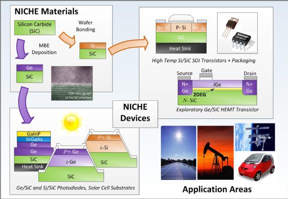
The Aim of the NICHE Project is to produce a new generation of silicon (Si) and germanium (Ge) electronic devices that can impact a variety of applications, by combining these materials with the high power, high temperature and ultra-hard material, silicon carbide (SiC). A wide bandgap semiconductor material of some repute itself, SiC is famed for its high temperature credentials, with a thermal conductivity as high as copper’s. On substrates of SiC, we are fabricating Si and Ge electronic devices such as transistors, diodes and indeed full integrated circuitry, that will all be provided with a performance boost as waste heat is efficiently transferred away from the active areas of each device. Furthermore, photodiodes, solar cells and photonic structures will be formed within exploratory Ge/SiC substrates.
The key Si/SiC Technology looks to have an impact on high temperature electronics, in applications such as down-hole drilling, space, electric cars and aerospace. This technology looks to improve the efficency of existing Silicon-on-Insulator (SOI) device architectures, which have already stretched Si device operation to 300°C. SOI uses a very thin layer of Si on an insulating silicon dioxide substrate that confines the semiconductor regions into a rigid space, restricting the amount of waste leakage current that can occur. However, a problem with SOI lies in the poor thermal conductivity of the insulating layer, making the extraction of waste heat difficult. By improving the thermal path of these devices by using the Si/SiC architecture we aim to push the power rating of Si devices at temperatures approaching 300°C, whilst providing a performance boost to power devices at any given operating temperature.
Ge/SiC Substrates permit a more exploratory set of devices, never before attempted. Photodiodes have shown significant initial promise with ultra-low dark currents. Similar structures are to be attempted in Si/SiC also.
Challenges
Several fascinating scientific challenges must be overcome during the NICHE Project, in the Materials Science of forming the layers, in the fabrication and optimisation of these new devices, in their high-temperature packaging, and in their characterisation.
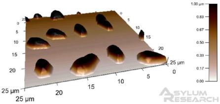
Forming layers of Ge or Si on SiC is tricky because their fundamental atomic structures are so different. Conventional epitaxy techniques such as MBE and CVD are the preferred ways of forming the Si/SiC and Ge/SiC substrates because of the intimate contact that will form between the layers as one material is deposited directly upon the other. However, as the material grows, the significant lattice mismatch (the difference in atomic spacing between the two materials) can cause distinctive islanding effects such as those shown below [P. M. Gammon, Development of SiC Heterojunction Power Devices]. Any layer that forms like this will be polycrystalline (having many areas of different crystal structure), will be very rough, and may not even cover the full growth area. Therefore, the growth conditions such as the temperature, pressure, rate and post growth treatments must be carefully controlled.
Another technique we can use to form our Si/SiC and Ge/SiC layers, is Wafer Bonding with its own balance of pros and cons.This technique is now commonplace within the silicon-on-insulator (SOI) industry, though it is a new and somewhat experimental approach when considering SiC. We will employ the SmartCut® process, where the Si and SiC are polished atomically flat and then forced together, allowing van der Waals forces to hold the wafers together. The Si, prior to bonding to the SiC will have been implanted sp that a large amount of hydrogen sits just below the surface. Heat treatment after the bonding causes the hydrogen to expand and crack the top Si layer off, leaving just a thin Si layer on the SiC. Unlike the MBE and CVD techniques, the wafer bonding leaves a solid, fully crystalline Si layer on the SiC, but is prone to having large air pockets and stray foreign partcles at the interface.
Acknowledgements
![]()
Collaborations
![]()