
Solar cells
Solar panels are devices made from semiconductors, of which silicon is currently the most widely used. Solar panels are a combination of single modules called solar cells that are electrically connected and whose function is producing electrical energy from solar light. This is done via the photovoltaic effect, defined as the absorption of the Sun’s light and its conversion into a current flowing between two oppositely charged layers.
Efficiency, the ratio of the electric power output to the light power input, and costs are the two most important criteria when investigating the suitability of the various materials for solar cells. The choice of the semiconductor defines the two main categories of technology: either crystalline silicon in a wafer form or thin films of other materials.
Physical operation principle of solar cells
In solar cell production, the silicon has impurities atoms introduced to create a p-type and an n-type region and thereby producing a p-n junction. However, p-n junctions of solar cells are not made by bringing a piece of n-type silicon into contact with a p-type, but rather, usually, by diffusing an n-type dopant into one side of a p-type wafer. By doing so, electrons from the n-type side of the junction, where their concentration is higher, diffuse towards the p-type side, where they recombine with holes. This migration of electrons leaves an excess of positive charge on the n-type side and causes an excess of negative charge on the p-type side, giving rise, as a consequence, to an electric field across the junction which acts as a diode. Electrons can move only in one direction: from the p-side to the n-side, but not the other way round, as shown in Fig. 1.
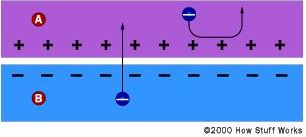
Fig. 1 Effect of the electric field in a solar cell. A: n-type silicon; B: p-type silicon. (Taken from Ref.[1]).
When light, in the form of photons, strikes the solar cell, electrons are promoted from the valence to the conductions band, thus creating electron-hole pairs. Any pair formed on or near the electric field separate, with electrons flowing in one direction and holes in the other to create a DC current, as depicted in Fig. 2.
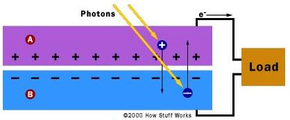
Fig. 2 General operation schematic of a solar cell. A: n-type silicon; B: p-type silicon. (Taken from Ref. [1]).
In a PV cell, photons are absorbed in the p layer. It's very important to "tune" this layer to the properties of the incoming photons to absorb as many as possible and thereby free as many electrons as possible. The solar radiation is composed of photons with different energies, but not all of them can excite electrons from the valence band to the conduction one. If the energy of the photon is lower than the band gap energy of the silicon semiconductor (about 1.1 eV for crystalline silicon), the photon passes straight through the silicon. On the other hand, when the photon energy is greater than the band gap of silicon, it is absorbed and its energy given to an electron in the crystal lattice. However, in the latter case, the difference in energy between these photons and the semiconductor band gap is converted into heat rather than into usable electrical energy, causing the loss of a certain percentage of the incident energy. Using materials with very low band gaps, in order to absorb more photons, is not beneficial since the band gap also affects the strength of the electric field across the junction and therefore, the voltage. Voltage and current determine the amount of power available from a solar cell, so the extra current gained by absorbing more photons due a reduced band gap, is lost because of a small voltage. The optimal band gap, balancing these two effects, is around 1.4 eV for a cell made from a single material.
The manufacturing process of a solar cell is completed with few more steps. Silicon is a very shiny material, which means that it is very reflective; however, photons that are reflected cannot be used by the cell. For this reason, as shown in Fig. 3, an antireflective coating is applied to the top of the cell to reduce reflection losses to less than 5 percent. The final step is the glass cover plate that protects the cell from the elements (rain, hail, etc.).
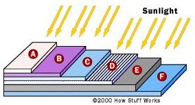
Fig. 3 Generic structure of a silicon solar cell. A: cover glass; B: antireflective coating; C: contact grid; D: n-type silicon; E: p-type silicon; F: back contact. (Taken from Ref. [1]).
Solar Cell Applications
There are many applications for solar cells. This section will focus on some interesting applications of solar cells that may be used in future. In figure 4, a car is powered exclusively by solar cells. Figure 5 illustrates flexible kind of solar cells which could potentially cover any shapes on homes and company buildings whilst providing them with electricity. Figure 6 shows a parking payment machine with a built in solar cell, visible in many town centres, and finally figure 7 shows solar cells integrated into clothing to provide electricity to small appliances such as mobile phones.
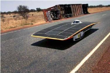
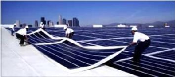
Figure 4: Solar Car Figure 5: Flexible solar cells


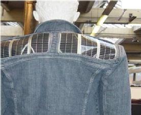
Figure 6: Payment machine powered by solar cells Figure 7: Clothes with integrated solar cells
References
[1] Website Sol http://science.howstuffworks.com/solar-cell3.htm
[2] Kwon 2008 Start of a New Generation: Nanotechnology in Solar Cells
[3] Elliot 2008 New Research on Semiconductors, Nova publisher, New York
Other sources consulted:
http://www.solarnavigator.net/solar_cells.htm