
2DM Electronic Structure
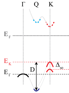
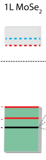
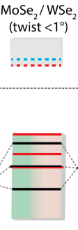
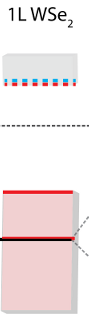
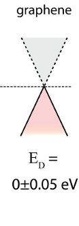
This page provides band parameters for monolayers and aligned heterobilayers of MoSe2 and WSe2, referenced to the Dirac point of an encapsulating layer of graphene.
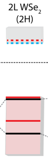
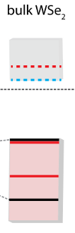
See the schematic for definitions of the parameters: Solid lines signify measured quantities; dotted lines DFT calculations.
The figure to the left provides a graphical illustration of the shifts of homologous bands and hybridization effects.
In both 2L WSe2 and heterobilayer MoSe2/WSe2, hybridization is almost undetectable at K (red bands) but much larger at (black bands). Table below: quantities determined by fitting the
-ARPES spectra.
 |
 |
 |
 |
 |
 |
 |
| EK (eV) |
-0.99 | -0.70 | -0.70 | -0.74 |
-0.79 |
|
| EK - E |
0.44 | 0.14 | 0.50 | 0.04 | -0.04 | |
| 0.24 |
- |
0.49 |
0.50 | 0.50 |
||
| D (eV) |
0.90 |
1.25 |
1.24 |
1.20 | 1.24 |
|
| m*K / m0 |
- | 0.4 |
0.4 |
0.5 | 0.4 |
|
| m* |
4.2 |
1.2 | 2.8 |
1.9 |
0.9 |
For reference, our calculated DFT (PBE) values of comparable quantities are shown below.
 |
 |
 |
 |
 |
 |
 |
| EK - E |
0.327 | -0.068 |
-0.247 | 0.485 |
0.049 |
-0.075 |
| 0.188 | 0.200 | 0.241 | 0.479 | 0.489 | 0.513 | |
| m*K / m0 | 0.625 | 0.610 | 0.603 | 0.425 | 0.428 |
0.426 |
| m* |
4.927 | 1.233 |
0.862 | 3.390 | 1.034 | 0.927 |
When making use of this information, please cite the following paper:
Band parameters and hybridization in 2D semiconductor heterostructures from photoemission spectroscopy
Neil R. Wilson, Paul V. Nguyen, Kyle L. Seyler, Pasqual Rivera, Alexander J. Marsden, Zachary P.L. Laker, Gabriel C. Constantinescu, Viktor Kandyba, Alexei Barinov, Nicholas D.M. Hine, Xiaodong Xu, David H. Cobden, Submitted (2016).