Request Epitaxial Growth
Please get in touch for your epitaxial and device processing requests. We are able to complete commercial contract of low volume wafers. Layers can be grown using pump prime funding for academic collaboration. Contact Vishal Shah for a consultation.
(UPDATE: Sept 2022) Pump-priming funding for SiC Epitaxy from Warwick is available from the UK National Epitaxy Facility.
Material Growth
- 4H-SiC on 4H-SiC growth (on-axis and off-axis)
- 6H-SiC on 6H-SiC growth
- 3C-SiC on Si
- Industry standard; Sizes up to 150mm wafer
- Thin, thick and super thick (0.1-120µm) epitaxial layers
- Multilayer (p(Al) and n(N)) in one run
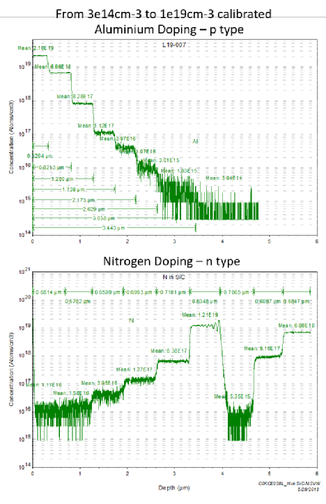
- Wide range of doping values (5e14cm-3 to 2e19cm-3)
- Feedback for defects, stress, crystallinity, surface roughness, carrier lifetime etc available.
- Physical characterisation using TEM, AFM, AFM, XRD techniques.
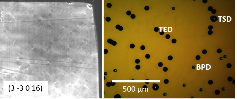
- Defect evaluation from molten-KOH can be performed.
- Experimental Semi-Insulating SiC layers can be incorporated
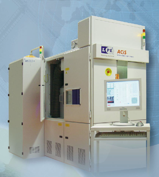
CVD Tool - LPE ACiS-M8
Thickness map over a 100mm 4H-SiC wafer
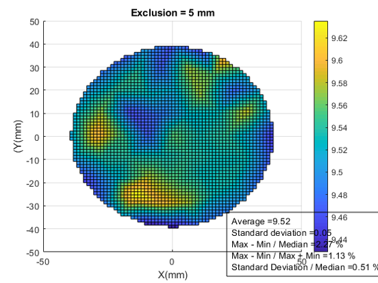
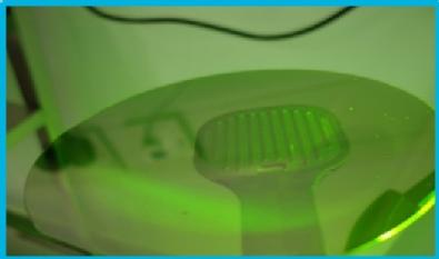
Image of a 4H-SiC wafer after growth
SIMS Measurements of doping achievable
Defect Analysis of a SiC wafer (right is XRDI, left are KOH pits)