
Equipment
We maintain an atomic layer deposition (ALD) facility and are core users of the Science City Cleanroom in the School of Engineering. We also have our own characterisation laboratories. We are regular users of various Research Technology Platforms at Warwick, including Electron Microscopy, Spectroscopy, X-Ray Diffraction, and X-Ray Photoemission Spectroscopy.
Atomic Layer Deposition
We have an Ultratech Fiji plasma-enhanced ALD system. Our standard precursors are Al, Si, Zn, Hf, and our standard co-reagents: H2O, O2 plasma, O3, N2 plasma.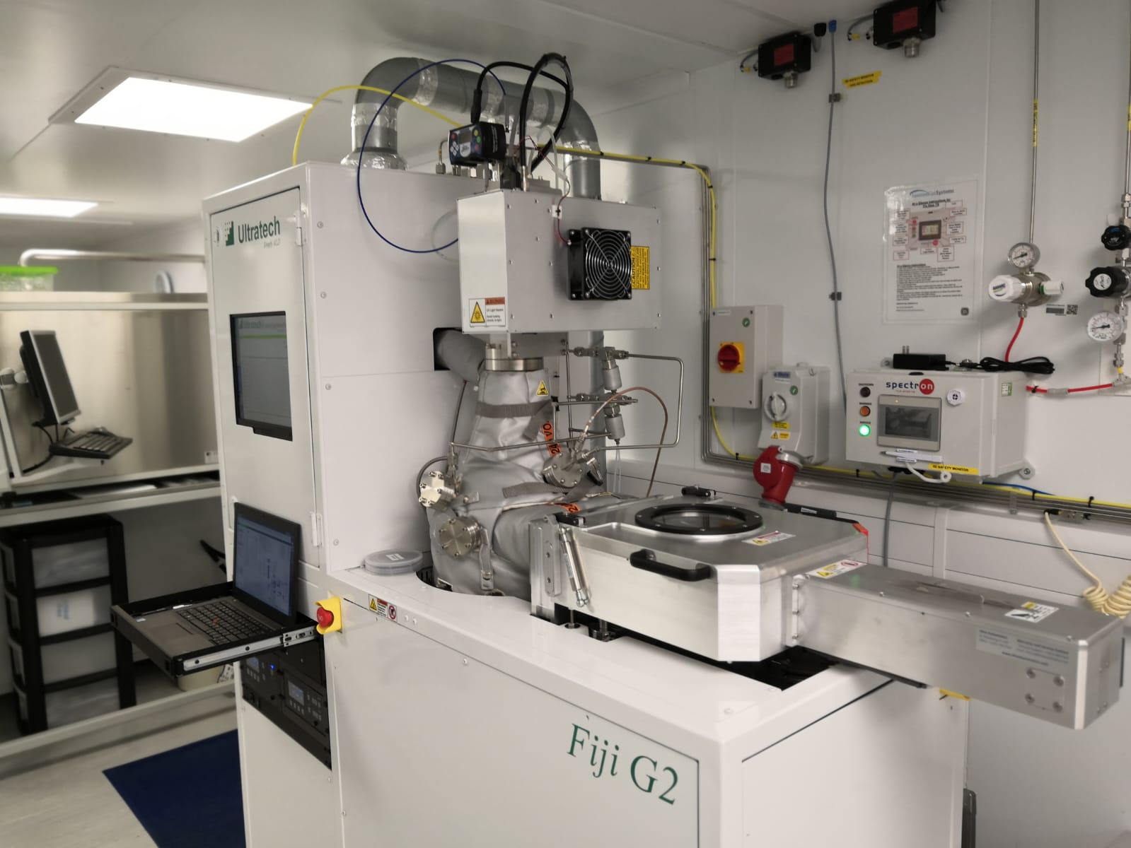
Battery Cycler
- It has 8 independent measurement channels with a maximum current of ±150 mA per channel, making it highly suited for small batteries such as coin cells.
- https://www.biologic.net/products/bcs-800/
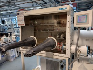
Gloveboxes
- We have two MBRAUN UNIlab modular gloveboxes with a gas purification system, solvent filter, and a controlled low-humidity atmosphere (<0.1 ppm of O2 and H2O). These are used for processing superacidic solutions and battery electrode materials
- We also have a lower specification glovebox for superacid passivation
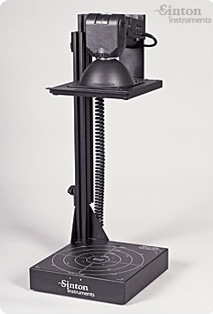
Photoconductance decay
- Quasi-steady-state photoconductance (QSS-PC). We have a Sinton
 Link opens in a new window WCT-120 lifetime tester, which enables the minority carrier lifetime to be determined as a function of the excess carrier concentration. In model system this can be used in a semi-spectroscopic manner to isolate fundamental properties of recombination-active defects. This system was modified by the manufacturer to fulfil our research requirements, and has a smaller coil than standard (1cm diameter). It is also possible to make temperature-dependent measurements (room temperature to ~150°C) using our system.
 - Quasi-steady-state photoluminescence (QSS-PL). Arriving in Summer 2014 will be a Sinton WCT-120PL system, which can also be used in QSS-PC mode. It can be used to determine minority carrier lifetime accurately at low levels of injection.
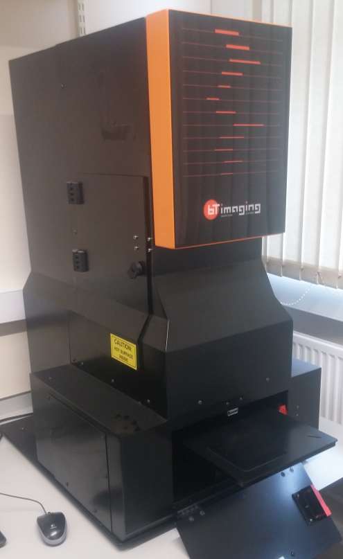
Photoluminescence Imaging
We have a a BT Imaging![]() Link opens in a new window LIS-L1 photoluminescence imaging system. This enables material quality images of whole wafers to be acquired within seconds. Under some conditions these maps can be calibrated in terms of the carrier lifetime and bulk interstitial iron concentration.
Link opens in a new window LIS-L1 photoluminescence imaging system. This enables material quality images of whole wafers to be acquired within seconds. Under some conditions these maps can be calibrated in terms of the carrier lifetime and bulk interstitial iron concentration.
Scanning Kelvin Probe
- Contact Potential Difference
- Surface Photovoltage
- 3D maps of surface potential
Other characterisation equipment includes two corona charging apparatus which can apply either positive or negative corona charge, and a