
VT Characteristics
When looking at the SSmS junction's VT behaviour (Figure 4) it is clear that at optimum operating voltage exists. In order to account for this one must consider the energy levels of a SSmS junction in the limit of a high applied voltage.
As depicted in figure 1, a voltage across the junction shifts the Fermi level in the semiconductor, allowing electrons with energy greater than (E-eV) to tunnel across into the empty states of the superconductor. If a voltage greater than 2Δ/e is applied, as in Figure 5 the Fermi level of the semiconductor is raised above the conduction band of the superconductor.
This allows electrons with energy below the Fermi level to escape through the junction, which raises the average temperature of the electron gas within the semiconductor, resulting in a net rise in temperature and negating any active cooling processes.
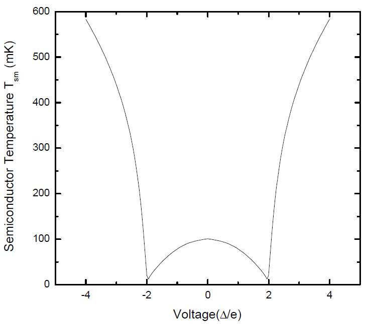
Figure 4: A voltage temperature plot of a typical SSmS cooling junction. The initial temperature of the device can be found by noting its temperature at an zero applied voltage.
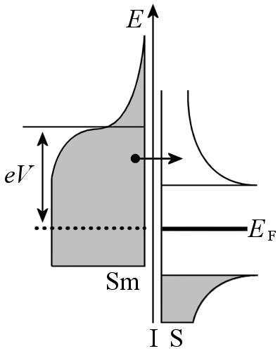
Figure 5: An energy level diagram depicting a cooling junction in the limit of a large bias voltage. The free states in the superconductor are now available to lower energy electrons.