
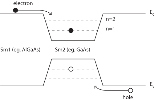
2DEGs and 2DHGs
Two-dimensional electron and hole gases (2DEGs and 2DHGs respectively) can be described as having quantised energy levels for one spatial dimension, but being free to move in the other two.
They can be produced by adjoining semiconductors with differently sized band gaps creating what is known as a Heterojunction.
| Figure 1: An energy level schematic of a heterojunction and the resulting square well. The wells created in the conduction and valence bands can be occupied by electrons and holes respectively, as shown. It is possible for an electron hole pair to combine and create a photon, the energy of which can be used to infer the structure of the energy levels within the wells. |
 |
Potential Wells
Depending on how heterojunctions are manufactured, the wells in which the 2DEGs and 2DHGs exist may have different forms such as square, triangular or parabolic.
For wells of infinite potential, the energy level solutions are as follows:
| Square: Triangular:
Parabolic: |
 |
 |
| where |
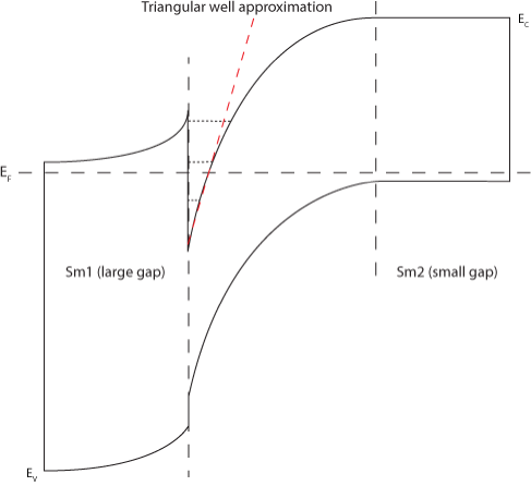
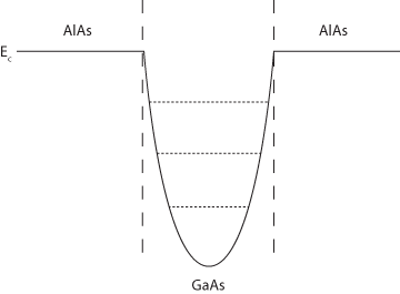
Triangular well | Parabolic well |
| Figure 2: An energy level schematic of a triangular and parabolic well. | ||
The triangular well approximation (shown in Figure 2) is widely used to describe electron energy bands at single heterojunctions. It allows the exact analytical solution of the Schrödinger equation (which must be solved self-consistently along with the Poission equation in order to determine the electronic structure at a heterointerface) in terms of Airy functions,
the eigenvalues of which describe the energy levels given above.
In practical calculations however, simpler, approximate analytic wave functions make calculations much more convenient. The simplest of these is the Fang Howard wave function.
where and
is determined by minimizing the total energy. This function however, does tend to overestimate the energy for the ground sub-band by around 6%.
A more accurate wave function is given by Takeda and Uemura,
which yields a ground sub-band energy only 0.4% larger than the exact Airy function value.
Solving the coupled Schrödinger and Poission equations (1D)
The Poisson equation shows that potential is directly related to charge density.
Schrödinger's equation is also related to the charge density, though not directly. Firstly we have the Schrödinger equation itself.
where is the electron wave function.
We note that the occupation of electronic states is given by the Fermi-Dirac distribution
which then allows the spacial density of electrons to be calculated using the solution of the Schrödinger equation (or an approximate solution, such as those mentioned above).
Where is the number of bound states.
We must now ask 'How does the charge density relate to the electron density
?' The answer is fairly straight forward once you consider the electron donors, which become positively charged and have density
This enables the Poisson equation to be re-written as
where is the permittivity of the material.
In order to solve Schrödinger and Poisson self-consistently, one starts with a trial potential and solves Schrödinger's equation.
is then calculated from the obtained wave functions and their corresponding eigenenergies. A second value of
may then be found from Poission's equation (using
and
). This second potential is then fed back into the Schrödinger equation and more iterations take place until
is less than a certain criteria.
A second example
In the following section we will consider a Si/SiGe heterojunction and the resulting 2DHG in oder to demonstrate a second method of describing the junction in terms of energy parameters and dopant concentrations.
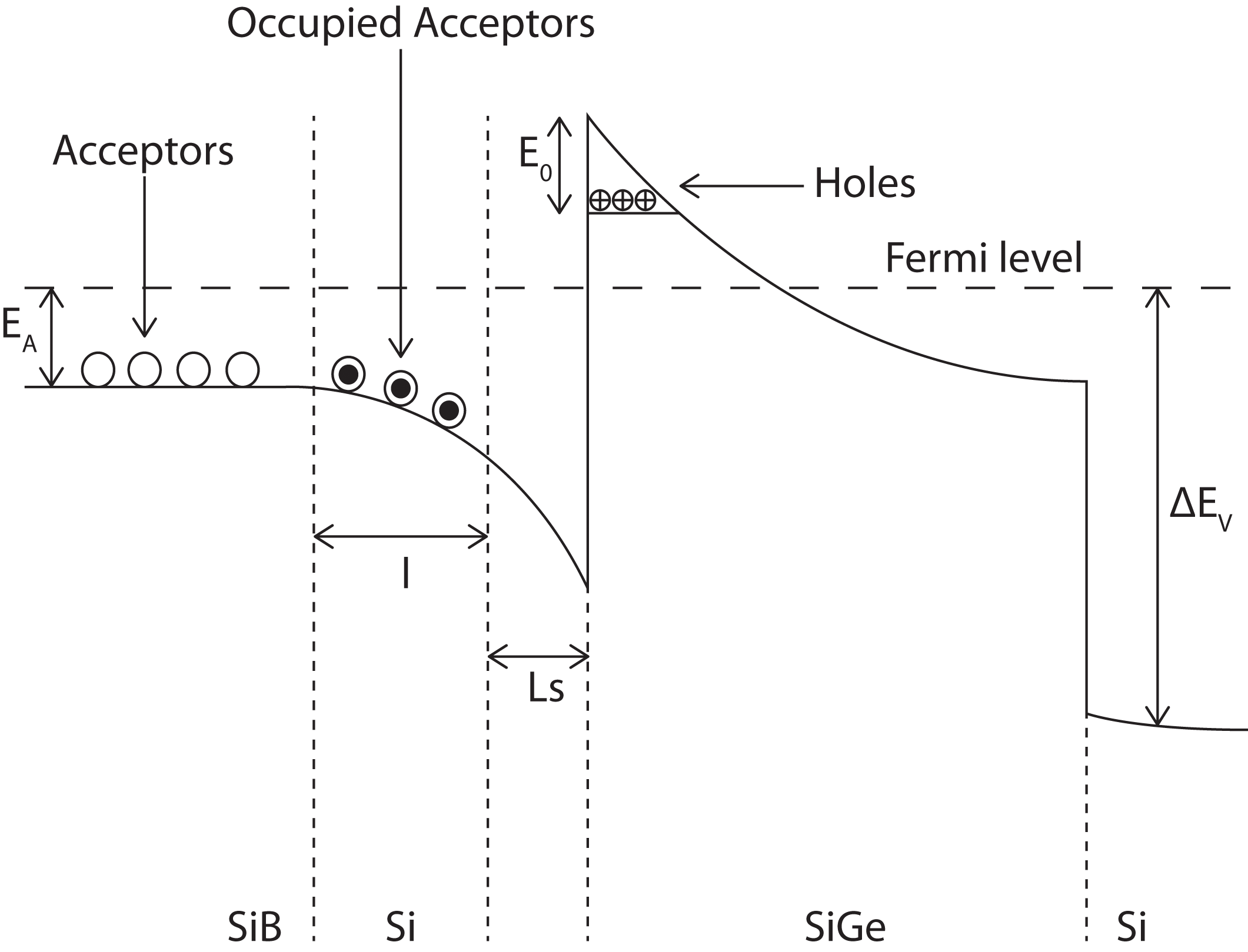 |
Figure 3: A simple schematic diagram of the valence band in a particular SiGe heterojunction. The sheet carrier density is obtained from the two-dimensional density of states for a single sub-band, and is given by (1) The electric field in the well is assumed to be uniform, allowing the triangular well approximation to be used, with the ground-state energy given by (2)
where |
with as the charge arising from background donor depletion within the SiGe alloy, the Si buffer later and the Si substrate. Allowing for the possibility of negatively charged impurities with sheet density
at the Si/SiGe interface, the electric field may also be written as
where is the acceptor concentration.
The set of equations can now be closed by adding all the potential variations from the bottom if the well up to the top of the valence band offset (3)
.
can then be found by choosing an initial value for
and solving (3) for
. This value is then compared to that given by equation (1) for this same Fermi energy. This method is repeated, moving along a range of
until the two yielded values of
are within a certain tolerance of each other, in much the same way as the previous example.
Bibliography
- S. M. Sze, Semiconductor Devices, John Wiley & Sons, 1985.
- J. H. Luscombe et al., Physical Review B 46 (1992).
- C. J. Emeleus et al., J. Appl. Phys 73 (1993).