
Dr Edward Butler-Caddle
I am a postdoctoral research fellow in the group of Dr. Rebecca Milot. I use time-resolved spectroscopy and s-SNOM (scattering-scanning near-field optical microscopy) to study charge carrier dynamics in semiconductors, with a focus on lead halide perovskite semiconductors for solar cells and LEDs.
Background:
I studied Natural Sciences (BA and MSci) at the University of Cambridge, specialising in physics. For my master’s project I investigated light-induced halide segregation of mixed-halide perovskites by studying the impact of using different ratios of precursor components, supervised by Dr Aditya Sadhanala.
I completed my PhD in physics at the University of Warwick (2023) under the supervision of Prof. James Lloyd-HughesLink opens in a new window, with a thesis titled "Time-resolved spectroscopy of charge-carrier dynamics in metal halide perovskites and other semiconductors for photovoltaics"Link opens in a new window. During my PhD I was a problems class teacher for "Mathematics for Physicists".
I am now a postdoctoral research fellow in the group of Dr. Rebecca MilotLink opens in a new window, where we are using an s-SNOM microscope (scattering-scanning near-field optical microscopy) that can study the optical properties and charge carrier dynamics on the nanoscale.
Research: Charge Carrier Dynamics in Metal-Halide Perovskites
I am investigating the charge carrier dynamics in metal-halide perovskites which is a class of semiconductors which show great potential for use in photovoltaic and light emitting applications.
I use time-resolved terahertz, time-resolved photoluminescence and time-resolved absorption spectroscopies to probe the carrier lifetimes and mobilities in these materials (see gifs on right).
Recently, I have started using an s-SNOM (scattering scanning near-field optical microscope) to measure optical properties on the nanoscale. Our s-SNOM microscope from NeaSpec is equipped with 532nm laser and visible and near-IR spectrometers, and we are adding a home-built time-resolved terahertz spectroscopy setup.
Published Work
Distinguishing carrier transport and interfacial recombination at perovskite-transport-layer interfaces using ultrafast spectroscopy and numerical simulation
Butler-Caddle et al., Physical Review Applied 22, 024013 (2024)Link opens in a new window (Editor's Suggestion)
During my PhD I used the spectroscopy techniques outlined above to observe the loss of charge carriers from the perovskite layer at the interface between a perovskite layer and a charge transport layer (CTL) deposited on top. Charge carriers may be lost from the perovskite, by either extraction or recombination, and to distinguish these loss mechanisms, a home-built drift-diffusion model was employed.
Terahertz photoconductance dynamics of semiconductors from sub-nanosecond to millisecond timescales
Butler-Caddle et al., Applied Physics Letters 122, 012101 (2023)Link opens in a new windowOptical pump terahertz probe spectroscopy (OPTP) can measure transient photoconductance decays with femtosecond temporal resolution (see below). However, its maximum temporal range is limited to only a few nanoseconds by the mechanical delay lines used. We extended the temporal range of OPTP to milliseconds and longer while retaining sub-nanosecond resolution. A separate pump laser was electrically synchronized to the probe pulses, allowing the pump–probe delay to be controlled with an electronic delay generator.High Bandwidth perovskite photonic sources on silicon
Ren, A., et al. Nature Photonics 17, 798–805 (2023)Link opens in a new window
Predicting solar cell performance from terahertz and microwave spectroscopy
H. Hempel et al., Advanced Energy Materials, 2102776 (2022)Link opens in a new window
Hot carriers in mixed Pb-Sn halide perovskite semiconductors cool slowly while retaining their electrical mobility
Monti et al., Physical Review B 102, 245204 (2020)Link opens in a new window
Approaching the Shockley-Queisser Limit for fill factors in lead-tin mixed perovskite photovoltaics
Jayawardena et al., Journal of Materials Chemistry A, 8 , 693-705 (2020)Link opens in a new window
THz spectroscopy
- Time-resolved THz spectroscopy involves measuring a short (almost single cycle) pulse of THz frequency radiation in the time domain, and observing how it changes when it passes through a sample. This can reveal information about the charge carrier density and mobility in the sample. Measuring in the time domain means both amplitude and phase information of the transmission spectrum is recorded.
- Optical pump terahertz probe (OPTP) spectroscopy can measure the conductivity and population of optically excited carriers as they evolve over time after optical excitation. This is done by comparing the transmission of the THz pulse through the sample with and without optical excitation of the sample.
Metal Halide Perovskites
- In the last decade there has been a dramatic surge of research into the properties and synthesis of metal-halide perovskites (MHPs), and their application in photovoltaic (PV) and light emitting devices.
- This interest is driven by the rapid rise in the efficiencies of solar cells based on these materials - reaching 25.2% (not stabilised) in 2019 [1]Link opens in a new window – coupled with the fact that the fabrication methods for MHPs are relatively simple, fast and inexpensive eg spin-coating from solution.
- The term Metal-Halide Perovskite actually refers to a broad range of materials which assume the perovskite crystal structure with an ABX3 composition where A is an organic or alkali metal cation, B is a metal ion and X is a halide ion. The X anion is typically I-, Br- or Cl-, the B cation is typically Pb2+ or Sn2+, and the A cation is typically methylammonium(+), formamidinium(+) or Cs(+). The broad range of possible compositions means there is a vast swathe of materials needing to be understood.
S-SNOM: scattering Scanning Near-field Optical Microscopy
> This technique uses metal tip of an atomic force microscope to measure the optical properties of a surface with a spatial resolution of tens of nanometres, which is independent of the wavelength. This spatial resolution is at least an order of magnitude better than the diffraction limit of half a wavelength, depending on the wavelength.> The metal tip acts as an antenna and a lightning rod for electromagnetic waves, resulting in an oscillating dipole in the metal tip that has a strong near-field surrounding it at the tip apex. The exact amplitude and phase of this oscillating dipole is affected by the properties of a sample placed within the near-field range of the tip, and thus the far-field radiation from this dipole is affected by the sample.

|
Position: Postdoc Supervisor: Group: |
Research Interests: perovskite semiconductors, THz spectroscopy, time-resolved spectroscopy, photoluminescence, solar cells, near-field microscopy
Funding: ERC
Contact
Email:
Office: Millburn House G40 (map)
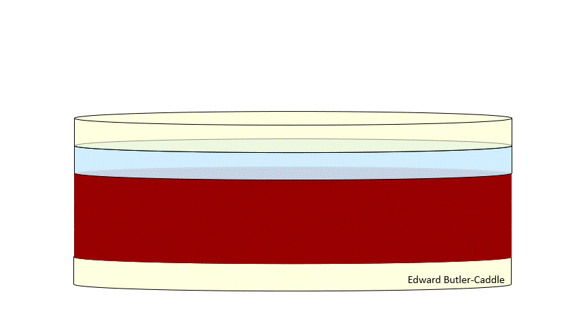
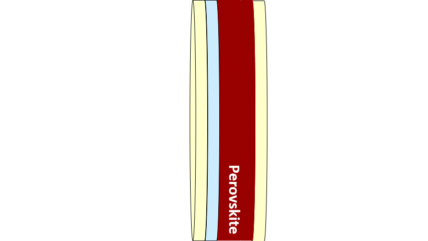
Above: A cartoon of measuring photoluminescence from a metal halide perovskite thin film. CTL is the charge transport layer used to extract electrons or holes (e- or h+).

Above: A cartoon of a transient absorption measurement of a metal halide perovskite thin film.
Above: A cartoon of an optical pump terahertz probe measurement of a metal halide perovskite thin film.