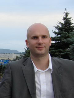
Dr. Maksym Myronov
PhD, MSc
Semiconductors Research Group Leader, Associate Professor
Maksym Myronov is a scientist, researcher, and inventor with expertise in epitaxial growth, materials characterisation, and device technologies involving group IV and III–V semiconductors. He has pioneered the use of group IV epitaxy to engineer novel nanoscale materials for a wide range of applications, including electronic, photonic, thermoelectric, spintronic, photovoltaic, quantum, energy storage, battery, and sensor devices. His work advances new frontiers at the intersection of physics, engineering, materials science, and quantum technologies.
Maksym has been collaborating with scientists, researchers and engineers from UK, Europe, USA, Asia and Japan establishing strong links with industrial and academic communities.
Strategic development of advanced semiconductor growth and microfabrication Infrastructure at the University of Warwick
- In 2008, he established SiGe Reduced Pressure Chemical Vapour Deposition (RP-CVD) growth capabilities at Warwick. Since then Maksym has been leading and developing them followed by expansion to Si-Ge-C-Sn and SiC epitaxial growth capabilities.
- In 2014, he led the expansion of the Physics Department’s cleanroom infrastructure, delivering additional state-of-the-art facilities with ISO 3 to ISO 7 classifications to support advanced research and microfabrication.
- In 2015, he led the installation and commissioning of the UK’s first Silicon Carbide (SiC) CVD system, significantly expanding Warwick’s epitaxial growth capabilities to include 3C-, 4H-, and 6H-SiC polytypes of wide band gap semiconductor materials.
- In 2019, he led the installation, commissioning, and establishment of research programmes for the Agile Microfabrication Facility within the Physics Department.
Research interests:
-
Science and technology of materials and solid state devices for applications in electronics, photonics, themoelectrics, photovoltaics, spintronics, cryogenics, sensors, Micro Electro Mechanical Systems (MEMS), Nano Electro Mechanical systems (NEMS), energy storage and quantum technologies.
-
Epitaxy of thin films and novel low-dimensional Group-IV semiconductors structures (Silicon (Si), Germanium (Ge), Diamond, Silicon Germanium (Si1-xGex), Silicon Carbon (Si1-xCx), Germanium Tin (Ge1-xSnx), Germanium Tin Silicon (Ge1-x-ySnxSiy), 3C-SiC, 4H-SiC, 6H-SiC etc) by Molecular Beam Epitaxy (MBE), Atomic Layer Deposition (ALD) and Chemical Vapour Deposition (CVD) techniques.
- Epitaxy of 2D materials (Germanene, Stanene, Silicene, Graphene etc).
- Epitaxy of III-V (InSb, InGaAs, GaN etc) semiconductors and their integration with Si.
- Epitaxy of semiconductors on Sapphire and SOI substrates
- Energy production, harvesting, storage and distribution.
Teaching:
- Physics of semiconductor materials and devices (since 2024)Link opens in a new window
- Fundamentals of semiconductor devices fabrication (2023)
- Introduction to microfabrication (since October 2019)
- Epitaxy fundamentals (since 2018)
- Epitaxial growth of the group-IV semiconductor materials (since 2011)Link opens in a new window
- Introduction to solid-state devices (since 2012)Link opens in a new window
Write To:
Department of Physics,
University of Warwick,
Coventry, CV4 7AL,
UK
Contact Details:
Office: P437 (inside of P432)
Telephone:
+44 (0) 2476 574383
E-Mail:
m.myronov@warwick.ac.uk
http://go.warwick.ac.uk/MaksymMyronov


