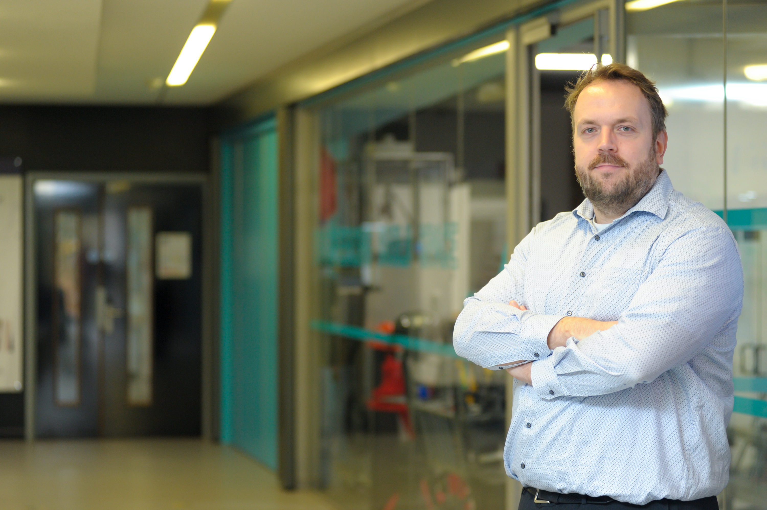
Dr Arne Renz

Dr Arne Benjamin Renz
Assistant Professor in Power Semiconductor Interfaces
Director of the Nanofabrication RTP at the University of Warwick
Electrical Power and Control Research Cluster Convenor
MSc, PhD, FHEA, MIEEE, MIET
arne dot renz at warwick dot ac dot uk
+447840264939
Biography
Dr Arne Benjamin Renz is an Assistant Professor and leading researcher in silicon carbide (SiC) power electronic interfaces at the University of Warwick's School of Engineering. Since his research career began in 2017, his research has focused on developing and commercialising novel ways of improving the power semiconductor interfaces that SiC forms with oxides (MOS) and metals (Schottky) for applications in EVs, renewable energy, the grid, satellites, and radiation-sensitive environments.
Dr Renz is currently Principal Investigator (PI) and co-Investigator (CI) on several highly competitive research grants, including Innovate UK/Switzerland Bilateral on "Innovations in SiC power MOSFET gate technology through the use of ALD oxides" (£1m total), and a CI on the REWIRE Innovation and Knowledge Centre (EP/Z531091/1), which aims to commercialise wide-bandgap semiconductor devices for power electronics in collaboration with over 30 industrial partners. He was lead researcher on major grants on radiation-hard SiC devices for space applications, including the SiCSAT Project (EP/V000543/1), and the development of ultra-high voltage (10 kV+) SiC IGBT devices for grid applications within the EPSPRC Centre for Power Electronics' Switch Optimisation Theme (EP/R00448X/1)
Research Interests
The market for SiC power devices was worth $2.7bn in 2023, a meteoric rise since the release of the first SiC MOSFET in 2011. This has been driven by demand from the electric vehicle, industrial machine, datacentre and renewable energy sectors. SiC’s fundamental properties include a high critical electric field, high thermal conductivity and wide bandgap compared to silicon. These properties underpin the fast switching and highly efficiency power converters, for which SiC has become known.
Despite this success, SiC has yet to reach its full potential. Silicon-based devices ranging from voltage ratings of 10V to nearly 10kV dominate most power electronic markets. By contrast, the breakthrough of SiC devices in the 600-1200V window is narrow and dominated by the fluctuating fortunes of the electric vehicle market.
The research conducted with Dr Renz' research area can be divided into two categories:
- Exploring New Applications for SiC: Developing novel interface technologies, especially focused on atomic layer processing (ALD/ALE), combining new processing avenues, seeks to open up avenues for mass-market power semiconductor devices. This includes trench architectures, use of recyclable semiconductor substrates, minimising channel losses in new 3-terminal switches such as SiC. My strong focus is on developing WBG-solutions for lower voltage applications, e.g., <600V.
- Advancing current interface technology: Dr. Renz is a leading researcher in SiC power semiconductor interfaces, blending materials science (oxide/gate/passivation chemistry) with practical device engineering (trench designs, superjunction architectures, reliability in radiation environments). His work is advancing next-generation high-voltage, high-reliability power electronics—critical for EVs, energy systems, and aerospace.
The research group prides itself in its close ties to industries. I have ongoing collaborations across the entire SiC supply chain - from material growers, chip manufacturers, equipment suppliers to automotive OEMs - ensuring that cutting-edge WBG interface technologies can transition from the "University world" to real-world applications.
Teaching Interests
ES3E0 - Power Electronics - Devices and Converters
ES2G1 - Power Electronics as a Degree Apprenticeship Module
ES3E7 - Power Systems and Electrical Machines
Publication
- The full and up-to-date list of publications are available on Google Scholar.
Projects and Grants |
|||
| Project title | Award | Year | Funder/Number |
| UP-SiC: Unlocking the Future Potential of SiC in Power Electronics | £2.5m | 2024-2027 | EPSRC |
| REWIRE IKC: Transforming Net Zero with Ultrawide Bandgap Semiconductor Device Technology Innovation and Knowledge Centre | £11m | 2024-2029 | UKRI |
| Innovations in SiC power MOSFET gate technology through the use of ALD oxides | £1m | 2024-2027 | Innovate UK/ InnoSuisse Bilateral |
| AdvanSiC: Advances in Cost-Effective HV SiC Power Devices for Europe's Medium Voltage Grids | £988k | 2022-2025 |
Horizon Europe 51611 |
| ASTEVA: Advancing SiC trench MOSFETs for future electric vehicles applications | £50k | 2023 |
EPSRC IAA 75915 |
| Research on novel SiC power device technologies for ultra-high-voltage applications | £20k | 2023-2025 | Royal Society International Exchanges Cost Share Jp. |
| SiCSat - Silicon Carbide Power Conversion for Telecommunications Satellite Applications | £746k | 2021-2024 |
EPSRC EP/V000543/1 |
| TraSiCA: High current 3.3kV SiC Schottky diodes for hybrid modules in traction applications | £500k | 2017-2018 |
Innovate UK 102897 |
Silicon carbide Facilities
The PEATER Group is one of the leading research groups in the world focused on SiC device development, with a suite of equipment and facilities to match. This includes:
- The Science City Cleanroom, a 150 m2 ISO class 6 cleanroom including high temperature oxidation and annealing furnaces, photolithography, etching and wet processing, metal deposition, and atomic layer deposition.
- The UK's only industrial SiC CVD reactor in an ISO class 4 cleanroom, used for the epitaxial growth of SiC.
- Characterisation Facilities, including a Keysight B1505A power device analyser and a SemiProbe semi-automated wafer prober for device characterisation up to 10 kV, 500 A and 300°C.
- An ISO class-8 packaging cleanroom.
