
Dr Vishal Shah

Dr Vishal Shah
Associate Professor
BEng, PhD, MInstP, MIET, FHEA
vishal dot shah at warwick dot ac dot uk
+44 (0) 24 7657 5467
 https://orcid.org/0000-0003-0232-4140
Biography
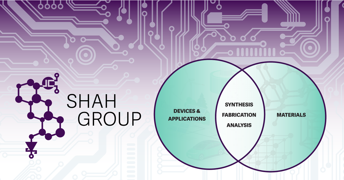
Dr Vishal Shah; Associate Professor, started the Shah Group at the School of Engineering at the University of Warwick in 2017 and is part of the PEATER group (Power Electronics Applications and Technology in Energy Research). He has been working in the wide bandgap (UWBG) materials research activity and his research interests are driven by the application-led materials development. He has over 15 years’ experience developing semiconductor materials and technologies for numerous application areas including power electronics, quantum technology, photovoltaics, CMOS, MEMS and sensing. He runs the materials development and characterisation activities of the group though the UK’s only Silicon Carbide (SiC) epitaxial facility at Warwick, and was the founder of the NanoFabrication RTP. He has written 5 patents, and published over 120 papers, five book chapters and made over 75 conference contributions, with an h-index of 21 and over 1568 citations (Google Scholar) as of Jan 2026. He is PI on a combined grant portfolio of £1.6M and CI on additional grants worth £18M.
Research Interests
4H-SiC Power devices and CVD Epitaxy: This activity is essentially based around the epitaxy of thick (>50µm) SiC layers for high power devices, developing fundamental materials synthesis projects. PhDs within the group are available in the topic. For example:
- Ultra high voltage (>10kV layers) on my fellowship EP/P017363/1 for HVDC technology.
- and 3D 4H-SiC epitaxy (EP/W004291/1)
Use of 3C, 4H and 6H-SiC materials in "More the Moore" applications: Is the next logical step for implementing other technologies using SiC knowledge from power electronics
- such as SiC for functional coatings (Innovate UK, 10073941))
- using SiC for photoelectrochemical generation of hydrogen from water splitting (funded from EPSRC EP/X527257/1)
- developing semi-insulating SiC for GaN integration for RF applications (CSHubJFS13 through EP/P006973/1)
- using 3C SiC as a MEMS material, developing material for SiC sensors etc.
Analysis and reduction of defects in semiconductors: We are developing new techniques for the detection of, reduction and utilisation of defects. For example, together with the Diamond Light Source we are developing non-destructive X-ray Diffraction Topography of materials and devices. In addition, we are developing DLTS measurement of point defects in either for use in quantum applications, or improve the efficiency of power electronics.
HeteroEpitaxy: Integration of different materials together for either added functionality, scaling of current technologies or for cost reduction.
- 3C-SiC on Si: Is an active an ongoing piece of research, 3C-SiC has the potential to be a biological material, sensing material and high temperature electronics as well. PhDs in our group to study this topic are available!
- Si on SiC: Deposition of doped Si and Ge on SiC substrates to create layers to be used in high temperature electronics. This investigation has involved a close collaboration with P.M.Gammon and the NICHE project, funded by the Royal Academy of Engineering.
- Si, strained-Ge on SiGe and Si: Has recently resulted in ultra-high carrier mobility structures, this research is funded by the Ge Renaissance program (EP/F031408/1) and the Si Photonics program (EP/E065317/1) and EPSRC grant EP/D034485/1.
Novel Device Fabrication Projects:
- Power Electronics Device Fabrication: The fabrication technology for SiC is a much more harsh and power intensive when compared to Si technology, requiring high temperature anneals, gas forming of 3D structures, high power etching and electrochemical etching. These techniques all need development to enable the next efficient power device!
- MEMS fabrication: This area of research is makes platforms which have a minimal volume and physically disconnected in a vacuum, meaning MEMS fabrication for suspended structures. Work from this programme has been submitted under two British patent applications: 1107574.4 and 1206913.4. This programme was funded by EPSRC grant EP/J001074/1
Device Characterisation: Utilising our state of the art device characterisation suite, we have been developing advanced Hall measurements, Deep Level Transient Spectroscopy (DLTS), Lifetime measurements to aid development of power electronic devices.
Projects and Grants
- 2025-2028 CI on £830k EPSRC network grant (EP/Z534432/1): UK Microsystems Network
- 2024-2029 CI on £12M EPSRC grant (EP/Z531091/1): Transforming Net Zero with Ultrawide Bandgap Semiconductor Device Technology (REWIRE)
- 2021-2025 PI on £400k EPSRC grant (EP/W004291/1Link opens in a new window): TESiC-SuperJ - Trench Epitaxy for SiC SuperjunctionsLink opens in a new window
- 2021-2024 CI on £975k EPSRC grant (EP/V028596/1Link opens in a new window): Electric Fields by 4D scanning transmission electron microscopyLink opens in a new window
- 2021-2024 CI on £740k EPSRC grant (EP/V000543/1Link opens in a new window): Silicon Carbide Power Conversion for Telecommunications Satellite ApplicationsLink opens in a new window
- 2017-2021 PI on £700k EPSRC Fellowship (EP/P017363/1Link opens in a new window): Ultra-high voltage (>30KV) power devices through superior materials for HVDC transmission (Wide Bandgap Epitaxy - SiC)Link opens in a new window
- 2019 PI on £60k EPSRC feasibility to develop semi-insulating epitaxy for monolithic integration of GaN RF and SiC Power devices. (CSHubJFS13 through EP/P006973/1)
- 2023 PI on £120k Henry Royce Materials Challenge Accelerator Programme, for “Developing 3C-SiC for Power Electronics and Photoelectrochemical Water Splitting” funded from EPSRC (EP/X527257/1)
- 2023 PI on £60k Innovate UK funding from Semiconductor scale up (10073941) “Feasibility study for SiC coatings”
- 2022-2027 CI on EU Horizon Grant agreement ID: 101075709, “AdvanSiC - Advances in Cost-Effective HV SiC Power Devices for Europe’s Medium Voltage Grids"
Selected Publications
For up to date lists please consult my Google Scholar, Scopus or ORCID
Research Facilities
The PEATER Group is one of the leading research groups in the world focused on SiC device development, with a suite of equipment and facilities to match. This includes:
- The NanoFab-RTP, a 150 m2 ISO class 6 cleanroom centre including high temperature oxidation and annealing furnaces, photolithography, etching and wet processing, metal deposition, and atomic layer deposition.
- The UK’s only industrial SiC CVD reactor in an ISO class 4 cleanroom, used for the epitaxial growth of SiC.
-
Characterisation Facilities, including a Keysight B1505A power device analyser and a SemiProbe semi-automated wafer prober for device characterisation up to 10 kV, 100 A and 300 °C.
-
An ISO class-8 packaging cleanroom.
Teaching
ES434 - ASICS, MEMS and Smart Devices
test
Group Page
Interested? Join us!
Office
F335Link opens in a new window
Advice and feedback hours
Office Hours: 9am – 5pm GMT. Student Hours: 2-3pm Wednesdays (term time) or by appointment.
Write to
School of Engineering, University of Warwick, Coventry, CV4 7AL.