
Defects on Si(100) surface
The analysis of defects on the Si(100) surface is important because they determine the morphology and, consequently, the quality of the surface. Important processes such as crystal growth, site of adsorption, and oxidation are reported to be undesirably influenced by the defects. In STM, some adsorbates are imaged similar to the defects.
“A”, “B” and “C” defects and their electronic nature
Fig. 1 shows the STM image of a Si(100) flat domain of 30x30nm2, imaged at -2.1V bias voltage and current setpoint I=20 pA. It is an example of the different types of defects observable on the Si(100) surface and the way they are distributed.
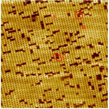
Fig. 1 Filled state STM image of Si(100) surface taken at a sample bias voltage of -2.1V, with a current setpoint I=20 pA over a scan area of 30x30 nm2.
The most common defects are known as “A”, “B” and “C” types, whose structural models are schematically illustrated in Fig. 2. “A” defects are vacancies in which two adjacent Si atoms are absent. Labelled as “A”, their presence is rather extended on the surface in Fig. 1. These missing dimer defects are also observed in pairs, forming double dimer vacancies, known as “B” defects and labelled as “B” in Fig. 1. When probing the filled surface states, type “C” defects appear like two adjacent Si atoms missing along the same direction resulting in two half-dimers, as in Fig. 2(c) [1]. In addition to the mentioned defects, other dimer vacancies clusters can be recognized on the Si(100) surface in Fig. 1. One of these, referred to as “split-off” dimers or 1+2-DV and circled in Fig. 1, consists of a single missing dimer neighbouring a cluster of two missing dimers [2]. Occasionally, clusters of more than two adjacent missing dimers appear.
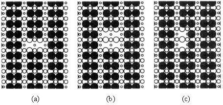
Fig. 2 Schematic model of three different type of defects detectable on Si(100) surface. (a) Type A single dimer vacancy defect; (b) type B double dimer vacancy defect; (c) type C defect. (Taken from Ref. [1]).
In Ref. [1] is also shown that the electronic nature of “A”, “B” and “C” defects can be probed by performing local tunnelling spectroscopy measurements to determine their I-V characteristics. This is the simplest form of STM tunnelling spectroscopy as well as the most straightforward way to demonstrate the semiconducting or metallic nature of the defects and, in general, of materials. The tunnelling I-V curves also provide information about the magnitude of the band gap: on a material with a surface state band gap, the tunnelling current falls exponentially to zero at a non-zero bias voltage.
In all I-V spectra in Fig. 3 the Fermi level is located at V=0. On the ideal silicon surface, Fig. 3(a), the current I drops to zero at ≈ -0.4 eV and ≈ 0.5 eV, which indicates that the band gap extends from ≈ 0.4 eV below the Fermi level to ≈ 0.5 eV above it. A similar semiconducting behavior is observed also on the single “A” defect, Fig 3(b), whose band gap is clearly visible, although reduced in magnitude on the unoccupied side of Fermi level where the current drops to zero at ≈ 0.2 eV. Type “B” defects are semiconducting too, even though the band gap is further reduced, as the current drops to zero at ≈ 0.2 eV also on the occupied side of the Fermi level, Fig. 3(c). Completely different characteristics are shown by “C” type defects, Fig. 3(d), whose I-V curve is an exponential function both above and below the Fermi level. This result demonstrates that “C” defects have a strongly metallic character, namely a high density of states near the Fermi level.
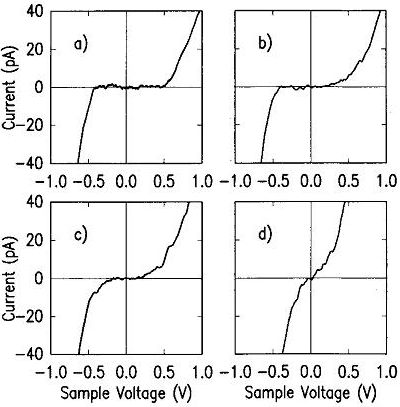
Fig. 3 Tunneling I-V curves measured on (a) ideal surface; (b) type A defect; (c) type B defect; (d) type C defect. (Taken from Ref. [1]).
Splitt-off or (1+2)-DV defects
The currently accepted atomic model to describe the split-off defects [2] is the one depicted in Fig. 4. This model represents the (1+2)-DV structure as a junction of a rebonded 1-DV with the unrebonded side of a 2-DV.
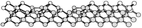
Fig. 4 Schematic model of the split-off dimer defect: the rebonded 1-DV is linked with the unrebonded side of a 2-DV. (Taken from Ref. [2]).
Boron-induced defects
Another type of defects commonly observed on Si(100) surfaces, especially when highly doped, is represented by the boron-induced defects. Boron is a widely used p-type dopant in silicon-based semiconductor technology; ultrahigh doping can be realized for B on Si substrates with a volume concentration of up to 25% [3]. When the sample preparation procedure is properly executed, the B atoms incorporated on a Si(100) surface can be recognized as protrusions. They are randomly distributed; most of them are paired, some single and some tripled, but they never appear combined in periodic structure.
An AFM image of Si(100) is proposed, Fig. 5, to better illustrate the features of a B-induced defect, which appears on the left-hand side as two bright protrusions. Each of them lies between two dimer rows, and four atoms belonging to adjacent rows are made undetectable.
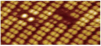
Fig. 5 qPlus AFM topographic image of Si(100) taken at 5nm oscillation amplitude (100 mV excitation), df setpoint of -4.9 Hz and applied sample bias of +0.1V. (Taken with A. Sweetman et al).
The model accepted for this type of defects [3] consists of an adsorbed dimer (A1 and A2) connecting two neighbouring rows to form a closed ring, as indicated in Fig. 6(a). The ring also includes the four hidden surface atoms (labelled with B), two atoms at the second layer (C1 and C2), and one atom at the third layer (D). Within each of these ring-shaped structures, boron atoms can be located at different positions, corresponding to different surface energy levels. However, the atomic configuration requiring the minimum surface energy is the one shown in Figs. 6(b)-(c), with one boron atom occupying an adsorbed dimer (A1) and two boron atoms at the second layer (C1 and C2), forming two symmetrical rings imaged as paired protrusions.
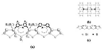
Fig. 6 Structural model proposed in Ref. [3] for the B-induced defect. (a) Symmetrical rings reproducing adsorbed dimers; (b) top view and (c) side view of the energetically favoured Si-B rings.
References
[1] R.J. Hamers, and U.K. Köhler, J. Vac. Sci. Technol. A 7 (4), 2854 (1989).
[2] Wang, J., Arias, T.A., and Joannopoulus, J.D., Phys. Rev. B 47 10497 (1993).
[3] Liu, Z., Zhang, Z., and Zhu, X., Phys. Rev. B 77 035322 (2008).