
MESFET
The acronym MESFET stands for "MEtal-Semiconductor Field-Effect Transistor". It is widely used in gallium arsenide technology since it does not require the growth of a quality oxide nor the tailoring of complex diffusion patterns which are fabrication techniques that are much harder to achieve in GaAs than in silicon. MESFETs can be operated at very high frequencies (>100 GHz) because they are based on high-mobility semiconductor materials and on fast-recovery Schottky diodes.
The MESFET is basically a JFET in which the width of the depletion region that pinches the channel is due to the presence of a Schottky diode instead of PN junction. A typical MESFET is realized in a thin semiconductor having a thickness a (Figure 1) and a doping concentration Nd. This layer is sitting on top of a lightly doped, high-resistivity semiconductor substrate. The substrate resistivity is so high that it is often referred to as a "semiinsulating" material. The substrate plays no active role in the device and simply acts as a mechanical substrate.
As in the case of the n-channel JFET the gate is biased with a negative voltage with respect to the source, which we will consider grounded. The gate voltage is used to modulate the width of the depletion zone, and therefore, the conductivity of the channel (Figure 1). The drain voltage is positive and higher than that of the source. The metal gate forms a reverse-biased Schottky diode with the N-type semiconductor, such that there is no gate current, except for a small leakage current.
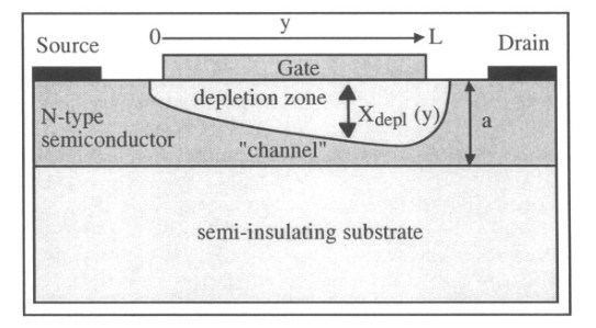
FIGURE1.Cross-section view of MESFET
If the drain voltage is small the width of the depletion zone can be obtained from the Schottky diode theory:
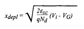
where Vi is the Schottky diode potential barrier on the semiconductor side and ¦ÅSC is the permittivity of the semiconductor. The threshold voltage is the gate voltage for which xdepl=a. Using the expressions above we find the threshold voltage:
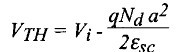
The threshold voltage can be either positive or negative, depending on the thickness of the N-type layer, the doping concentration Nd and the metal used to form the Schottky gate. If the threshold voltage is negative the ESFET is a depletion-mode device; if it is positive, it is an enhancementmode MESFET.
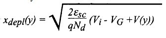
The current in the MESFET can be calculated as a function of gate and drain voltage using a technique similar to that which was used for the JFET. Since the channel basically behaves as a resistor the current flow from source to drain gives rise to a progressive potential drop along the channel. The potential in the channel, noted V(y), varies from V(y=0)=VS=0 at the source to V(y=L)=VD at the drain. In each vertical section located at a position y the reverse bias across the Schottky junction is, therefore, equal to VG-V(y).As a consequence the width of the depletion zone varies as a function of y in such a way that:
The expression for the current is obtained by integrating Ohm's law from source to drain:
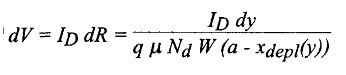
where W is the device width.
Replacing xdepl(y) by its value we obtain:
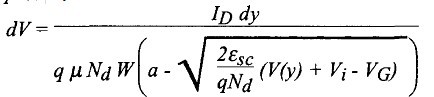
which can be re-written as:
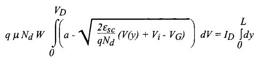
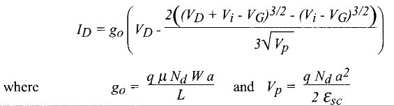
Performing the integration we obtain the Drain Current:
These equations are valid if the channel is not pinched-off, i. e. if the device is not in saturation. Pinch-off occurs when xdepl(L)=a, at which point VD=VDsat=VP-Vi+VG.
Saturation Drain Voltage:VDsat=VP-Vi+VG=VG-VTH.
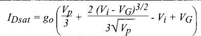
The drain saturation current is obtained by replacing VD by the saturation drain voltage VDsat, in Expression above, which yields the saturation drain current:
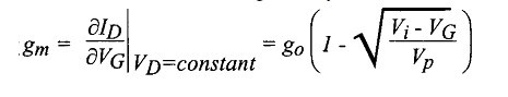
The transconductance in saturation is given by:
References
1 S.M. Sze, Physics of semiconductor devices, J. Wiley & Sons
2 R.S. Muller and T.I. Kamins, Device electronics for integrated circuits, J.Wiley and Sons
3 J-P Colinge and C.A. Colinge, Physics of semiconductor devices, Kluwer academic publishers