
MOSFET
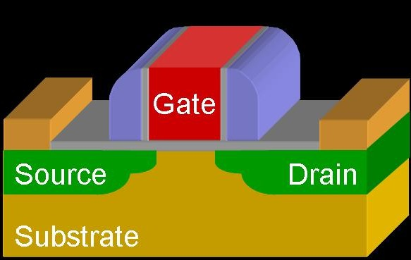
MOSFETThe metal-oxide-semiconductor-field-effect-transistor (MOSFET) is a vital device used in integrated circuits for many applications, ranging from power supplies to memories. A skectch of a MOSFET is shown below:
The parameters that define it are:
The MOSFET has 3 modes of operation. The cut off mode, in which there is no current flow throughout the drain since the gate voltage is lower than the drain and source voltage. If we apply a small voltage in the drain electrons will flow from the source to the drain, the current now is different from zero. The conducting channel acts as a resistor, this is the linear region. If we continue to increase the voltage we will get out of this region, since the increase in the voltage is balanced with the decrease in the charge. beyond the point Qn~0 ( pinch-off point) the drain current remains unchange and we enter the saturation regime.
At the moment, the goal is to scale down the MOSFET since we are entering in a new era of even smaller devices. Ideally we could scale down all parameters and the applied voltages with the same scaling factor k and increase the doping profile by k; this would lead to an unchanged threshold swing. However this can’t be done due to physical and technological limitations. However, there are some physical and technological limitations, such us:
Due to all limitations other scaling models have been proposed: constant-voltage scaling, quasi-constant-voltage scaling, generalized scaling and flexible scaling factor. In the last one, we can change specific parameters independently as long as the general behaviour remains the same. Also the advance of some technologies have given a help, such the use of high-k dielectrics for gate dielectrics which can relax the physical thickness improving the defect density and reducing the field for tunnelling; MOSFET built on a very thin body 3D structure will decrease significantly the conduction path for punch-through.
|
|
-
High K dielectric:
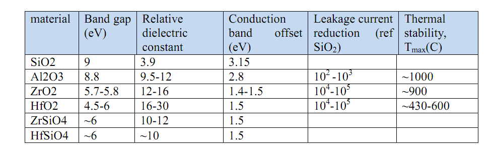
As part of device scaling in silicon, the oxide thickness must be reduced to a few nm. Scaling the oxide thickness leads to a significant amount of leakage current due to tunnelling. For that reason, new high k dielectric materials instead of SiO2 are required. However, the narrower band gap of high-k materials cancels the benefit of the high dielectric constant. Therefore, a suitable trade-off between the dielectric constant and the conduction band offset is the first criterion for high-k dielectric candidates need . A few high-k dielectrics show the promise to replace silicon dioxide, and some of their fundamental parameters are listed in the following Table which it appear that SiO2 has the lowest dielectric constant.
-
Short channel effect:
As the channel length is reduced the Drain influence becomes stronger. As a result, it becomes harder for the gate to control the source barrier and turn off the channel. To control short channel effects, halo doping or implantation has been introduced that reduces the drain-induced barrier lowering (DIBL), section at higher drain to source bias Vds.
There are several parameters that are affected by short channel effect:
-
Punchthrough and Drain Induced Barrier Lowering
-
Velocity Overshoot .
-
Threshold Voltage Roll-off.
-
Impact ionization and Hot Electrons.
-
Gate Leakage .
-
Surface scattering:
-
Strain:
Applying strain to Si or Ge channel has been demonstrated to provide significant performance advantages which enhance mobility of carriers in devices without having to change the basic channel material .strain also reduces the band gap of the semiconductor that may increase band to band tunnelling (BTBT) that is responsible for the off current,confinement on the other hand leads to an increase in band gap energy and reduces (BTBT) leakage. Therefore a trade off between these two components should be taken to enhance mobility. Strain also affect the carrier effective mass, velocity and reduce the interval scattering which
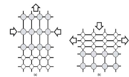
improve the carrier mobility.The notion of placing the channel of a CMOS device under strain has been in the scientific community since 2001 that it had developed a new form of silicon. Strained Silicon (S-Si) is achieved by either increasing (tensile) or reducing (compressive) the atomic spacing between the Si atoms in the Figure . The type of strain is described relative to the x and y planes of the device channel. If stress is applied to:
One axis → unaxial strain
Two axis → biaxial strain see the figure
references
1- A. Dobbie, Investigation of the Electrical Properties of Si1-xGex channel pMOSFETs with High-k Dielectrics, PhD Thesis University of Warwick 2007.
2- Xingsheng Wang, Simulation Study of Scaling Design, Performance Characterization, Statistical Variability and Reliability of decananometer MOSFETs, university of
Glasgow May 2010.
3- David Leadly, Novel Materials for Nanoscale CMOS 3,chapter 1,2007.