
STM-Scanning Tunneling Microscope
The scanning tunneling microscope was invented in 1981 by Gerd Binnig and Heinrich Rohrer. Using STM, in 1982 they obtained for the first time real-space images of atomic structures of Si(111)-7x7 reconstructed surface [1], and for their invention of STM, in 1986 they were awarded the Nobel Prize.
The STM is a non-optical electron-based microscope which employs the quantum mechanical effect of tunneling. It works by scanning a very sharp metal tip over a conducting surface within a range of several angstroms of it. When the tip is brought to such a close distance from the sample and a bias voltage is applied between the tip and the sample, a tunneling current flows through the vacuum gap that separates the two conductors, even though they are not in electrical contact. Fig.1 shows the general setup of an STM. The tip is mounted on a piezotube which undergoes a mechanical deformation because of the applied electric field. As a consequence, the position of the tip is locally changed along the lateral and vertical direction. The set point value for the current is determined by the user. During normal operation, the tunneling current is held constant through the use of a feedback circuit. Once a stable tunnel junction is achieved, the tip is raster scanned over the surface and its position is varied via the distortions of the piezoelectric actuator, so that the current remains constant. When this operating mode is used, images are created recording the vertical position required to keep the current constant. These images contain information about the geometry and electronic structure of the surface, revealing the real-space structure of the surface under investigation. The vertical resolution in scanning tunneling arises from the extremely high sensitivity of the tunneling current with respect to the tip-sample distance.
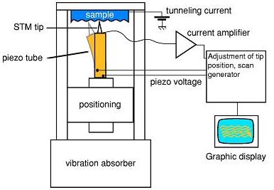
Fig. 1 Schematic illustration of an STM. (Taken from Ref.[2]).
Qualitatively, it can be described by referring to the energy diagram of a tunneling gap, as depicted in Fig.2. The potential barrier in the vacuum range between the two systems determines the decay of surface wave functions in the same range. When the applied voltage is small compared to the work function Φ of the two surfaces, the tunneling barrier is approximately rectangular with a width z and height given by the work function.
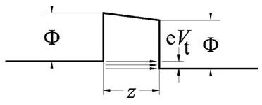
Fig. 2 Energy diagram of an ideal tunneling gap. (Taken from Ref. [3]).
The current then decays exponentially with a constant exponent, which is proportional to Φ and z:
where I0 is a function of the applied voltage and density of states in both tip and sample, m is the mass of the electron and ħ is the reduced Planck’s constant [3]. When the voltage bias is no longer negligible, the effective barrier height Φ-eVt is to be considered.
It is worth pointing out that an STM image is not directly related to the nuclear position of surface atoms, but it is a map of the spatial variation of the density of electronic states at the surface, within the energy window defined by the tip/sample bias.
Since electrons can flow from the metal tip to the sample surface or vice versa, depending on the polarity of the bias, it is possible to gain more information about the electronic structure of the surface by studying the variation of the STM signal on the sign and magnitude of the tip-sample voltage. The applied bias shifts the relative position of the Fermi level and makes available unoccupied states in an energy window in which electron tunneling can occur. This is qualitatively shown for opposite bias voltages in the electronic-band plots in Fig. 3. When the tip is negatively biased with respect to the conductive sample, electrons can only tunnel from occupied states of the tip into empty states of the surface, in the energy window eV.
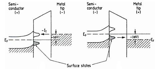
Fig. 3 Energy band scheme of the tunneling junction for two opposite values of bias voltage. Flow of electrons from the tip into empty surface states (left-hand side), and from filled surface states into the metal tip (right-hand side). (Taken from Ref. [4]).
On the other hand, when the tip is positively biased, tunneling of electrons from the metal into the sample surface does not occur. Because of the Fermi-level position, the measured tunneling current originates in this case from occupied surface or valence-band states in the sample. Therefore, depending on the bias direction, occupied or empty states of the surface under investigation can be probed [4].
References
[1] G. Binnig, H. Rohrer, Ch. Gerber, and E. Weibel, Physical Review Letters, vol. 50, no. 2, pp. 20-123, 1983.
[2] W.A. Hofer, A. Foster and A. Shluger, Reviews of Modern Physics, 2003, 75(4): p. 1287-1331.
[3] F.J. Giessibl, Advances in atomic force microscopy, Rev. Modern Phys., 75 (2003), pp. 949–983.
[4] Lüth H. Surfaces and Interfaces of Solid Materials (3rd edn). Springer: