
Scanning Electron Microscopy (SEM)
Scanning electron microscopes use a beam of highly energetic electrons to examine objects on a very fine scale. In a SEM, when an electron beam strikes a sample, a large number of signals are generated. Secondary electrons (SE) are produced when an incident electron excites an electron in the sample and loses some of its energy in the process. The excited electron moves towards the surface of the sample and, if it still has sufficient energy, it excites the surface and is called a secondary electron (non-conductive can be coated with a conductive material to increase the number of the secondary electrons that will be emitted with energies less than 50 eV).
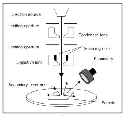
Figure 1 Schematic diagram of an SEM set-up [1]

Figure 2 A new field-emission SEM, the Hitachi SU-70 Schottky field emission SEM, with analytical (EDS) capability provides many special features such as dual secondary electron detector system, high probe current, beam deceleration, field free mode for EBSD and magnetic samples and low kV backscattering electron imaging. These special features will enable users to investigate and characterise nanomaterials (both nanostructure imaging as well as microchemical analysis) in great detail [2].
References:
1. Kourosh Kalantar-zadeh, B.F., Nanotechnology-Enabled Sensor: Springer; 1 edition (October 31, 2007).
2. http://www.nanocenter.umd.edu/new_facilities/NispLab.php
Bibliography:
1. Scanning Electron Microscopy and X-ray Microanalysis by Joseph Goldstein, Dale E. Newbury, David C. Joy, and Charles E. Lyman
2. Scanning Electron Microscopy: Physics of Image Formation and Microanalysis (Springer Series in Optical Sciences) by Ludwig Reimer