
SEM
Scanning Electron Microscopy (SEM)
Scanning electron microscopes use a beam of highly energetic electrons to examine objects on a very fine scale. In a SEM, when an electron beam strikes a sample, a large number of signals are generated.
This examination can yields the information such as topography (the surface features of an object), composition (the elements and compounds that t=the object is composed of and the relative amounts of them) and crystallographic information (how the atoms are arranged in the object). The combination of high magnification, large depth of focus, good resolution, and the ease of observation makes the SEM one of the most widely uses equipments.
Secondary electrons (SE) are produced when an incident electron excites an electron in the sample and loses some of its energy in the process. The excited electron moves towards the surface of the sample and, if it still has sufficient energy, it excites the surface and is called a secondary electron (non-conductive can be coated with a conductive material to increase the number of the secondary electrons that will be emitted with energies less than 50 eV).
Alternatively, when the electron beam strikes the sample, some of the electrons are scattered (deflected from their original path) y atoms in the specimen in an elastic fashion (no loss of energy). These essentially elastically scattered primary electrons (high-energy electrons) that rebound from the sample surface are called backscattered electrons (BSE).
The mean free path length of secondary electrons in many materials is 10 Ǻ. Thus, although electrons are generated throughout the region excited by the incident beam, only those electrons that originate less than 10 Ǻ deep in the sample escape to be detected as secondary. This volume of production is very small compared with BSE and X-rays. Therefore, the resolution using SE is better than either of these and is effectively the same as the electron beam size. The shallow depth of production of detected secondary electrons makes them ideal for examining topography. The secondary electron yield depends on many factors, and is generally higher for high atomic number targets, and at higher angles of incidence.
BSE can be used to generate an image in the microscope that shows the different elements present in a sample. All elements have different sized nuclei and as the size of the atom nucleus increases, the number of BSE increases; therefore, the backscattered electron image contains two types of information: one on specimen composition and the other on specimen topography. BSE emission intensity is a function of the specimen’s atomic number, therefore, the higher the atomic number, the brighter the signal. For example, minerals with 26 Fe will appear brighter than 12 Mg.
The generation region of backscattered electrons is larger than that of the secondary electrons, namely, several tens of nm; therefore backscattered electrons give poorer special resolution than secondary, they are less influenced by charge-up.
In conjunction with the scanning electron microscopy, energy dispersive x-ray spectroscopy (EDS or EDX) is technique that utilizes X-ray emitted from the sample during the bombardment by the electron beam to characterize the elemental composition of material imaged in a SEM. When the sample is bombarded by the electron beam of the SEM, electrons are ejected from the atoms comprising the surface of sample. A resulting electron vacancy is filled by an electron from a higher shell, and an X-ray is emitted to balance the energy difference between the two electrons. The EDX X-ray detector measures the number of emitted X-ray versus their energy. The energy of the X-ray is characteristic of the element from which the X-ray was emitted. A spectrum of the energy versus relative counts of the detected X-ray is obtained and evaluated for qualitative and quantitative determination of the elements present in the sampled volume.
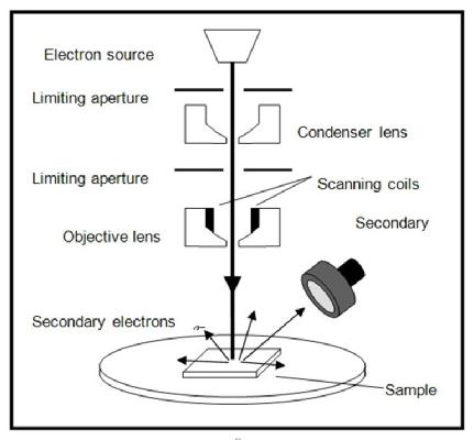
Figure 1 Schematic diagram of an SEM set-up [1]

Figure 2 A new field-emission SEM, the Hitachi SU-70 Schottky field emission SEM, with analytical (EDS) capability provides many special features such as dual secondary electron detector system, high probe current, beam deceleration, field free mode for EBSD and magnetic samples and low kV backscattering electron imaging. These special features will enable users to investigate and characterize nanomaterials (both nanostructure imaging as well as microchemical analysis) in great detail [2].
Refernces:
1. Kourosh Kalantar-zadeh, B.F., Nanotechnology-Enabled Sensor: Springer; 1 edition (October 31, 2007).
2. http://www.nanocenter.umd.edu/new_facilities/NispLab.php
Bibliography:
1. Scanning Electron Microscopy and X-ray Microanalysis by Joseph Goldstein, Dale E. Newbury, David C. Joy, and Charles E. Lyman
2. Scanning Electron Microscopy: Physics of Image Formation and Microanalysis (Springer Series in Optical Sciences) by Ludwig Reimer