
Transmission Electron Microscopy (TEM)
TEM
The transmission electron microscope is a very powerful tool for material science. A high energy beam of electrons is shone through a very thin sample, and the interactions between the electrons and the atoms can be used to observe features such as the crystal structure and features in the structure like dislocations and grain boundaries. Chemical analysis can also be performed. TEM can be used to study the growth of layers, their composition and defects in semiconductors. High resolution can be used to analyze the quality, shape, size and density of quantum wells, wires and dots.
The TEM operates on the same basic principles as the light microscope but uses electrons instead of light. Because the wavelength of electrons is much smaller than that of light, the optimal resolution attainable for TEM images is many orders of magnitude better than that from a light microscope. Thus, TEMs can reveal the finest details of internal structure - in some cases as small as individual atoms.
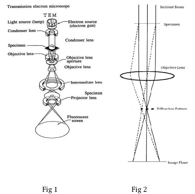
Figure 1 - General layout of a TEM describing the path of electron beam in a TEM (Taken from JEOL 2000FX Handbook)
Figure 2 - A ray diagram for the diffraction mechanism in TEM
Imaging
The beam of electrons from the electron gun is focused into a small, thin, coherent beam by the use of the condenser lens. This beam is restricted by the condenser aperture, which excludes high angle electrons. The beam then strikes the specimen and parts of it are transmitted depending upon the thickness and electron transparency of the specimen. This transmitted portion is focused by the objective lens into an image on phosphor screen or charge coupled device (CCD) camera. Optional objective apertures can be used to enhance the contrast by blocking out high-angle diffracted electrons. The image then passed down the column through the intermediate and projector lenses, is enlarged all the way.
The image strikes the phosphor screen and light is generated, allowing the user to see the image. The darker areas of the image represent those areas of the sample that fewer electrons are transmitted through while the lighter areas of the image represent those areas of the sample that more electrons were transmitted through.
Diffraction
Figure 2 shows a simple sketch of the path of a beam of electrons in a TEM from just above the specimen and down the column to the phosphor screen. As the electrons pass through the sample, they are scattered by the electrostatic potential set up by the constituent elements in the specimen. After passing through the specimen they pass through the electromagnetic objective lens which focuses all the electrons scattered from one point of the specimen into one point in the image plane. Also, shown in fig 2 is a dotted line where the electrons scattered in the same direction by the sample are collected into a single point. This is the back focal plane of the objective lens and is where the diffraction pattern is formed.
Specimen Preparation
A TEM specimen must be thin enough to transmit sufficient electrons to form an image with minimum energy loss. Therefore specimen preparation is an important aspect of the TEM analysis. For most electronic materials, a common sequence of preparation techniques is ultrasonic disk cutting, dimpling, and ion-milling. Dimpling is a preparation technique that produces a specimen with a thinned central area and an outer rim of sufficient thickness to permit ease of handling. Ion milling is traditionally the final form of specimen preparation. In this process, charged argon ions are accelerated to the specimen surface by the application of high voltage. The ion impingement upon the specimen surface removes material as a result of momentum transfer
References
Transmission electron microscopy, David B. Williams and C. Barry Carter (Plenum, 1996)
Electron microscopy of thin crystals, Peter Hirsch (Butterworths, 1965)