
Hall Effect Measurements
Electrical characterization of materials evolved in three levels of understanding. In the early 1800s, the resistance R and conductance G were treated as measurable physical quantities obtainable from two-terminal I-V measurements (i.e., current I, voltage V). Later, it became obvious that the resistance alone was not comprehensive enough since different sample shapes gave different resistance values. This led to the understanding (second level) that an intrinsic material property like resistivity (or conductivity) is required that is not influenced by the particular geometry of the sample. For the first time, this allowed scientists to quantify the current-carrying capability of the material and carry out meaningful comparisons between different samples. Theories of electrical conduction were constructed with varying degrees of success, but until the advent of quantum mechanics, no generally acceptable solution to the problem of electrical transport was developed. This led to the definitions of carrier density n and mobility µ (third level of understanding) which are capable of dealing with even the most complex electrical measurements today.
The Hall Effect and the Lorentz Force
The basic physical principle underlying the Hall effect is the Lorentz force. When an electron moves along a direction perpendicular to an applied magnetic field, it experiences a force acting normal to both directions and moves in response to this force and the force effected by the internal electric field. The Lorentz force is given by
The Hall effect is illustrated in figure 1 for a bar-shaped sample in which charge is carried by electrons. A constant current I flows through the bar and the entire bar is subject to a uniform magentic field B, which is directed into the screen, perpendicular to the current flow. Since the electrons are travelling through a magnetic field, they are subject to an upwards Lorentz force and so drift to the top of the bar whilst maintaining their horizontal motion. This leads to a build up of negative charge on one side of the bar and positive charge on the other due to the lack of electrons. This leads to a potential difference between the two sides of the sample, that can be measured as the Hall voltage VH. (Note that the force on holes is toward the same side because of their opposite velocity and positive charge.)
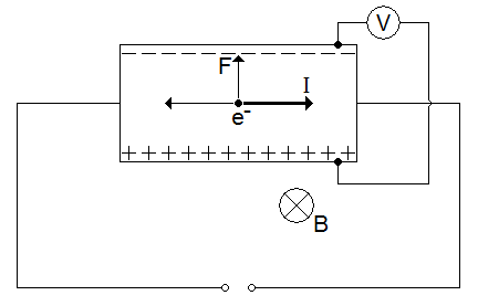
Figure 1: Illustration of the Hall effect in a bar of conducting material.
This transverse voltage is the Hall voltage VH and its magnitude is equal to IB/qnd, where I is the current, B is the magnetic field, d is the sample thickness, and q (1.602 x 10⁻¹⁹ C) is the elementary charge. In some cases, it is convenient to use layer or sheet density (ns = nd) instead of bulk density. One then obtains the equation
(1)
Thus, by measuring the Hall voltage VH and from the known values of I, B, and q, one can determine the sheet density ns of charge carriers in semiconductors. If the measurement apparatus is set up as shown, the Hall voltage is negative for n-type semiconductors and positive for p-type semiconductors. The sheet resistance RS of the semiconductor can be conveniently determined by use of the Van der Pauw resistivity measurement technique. Since sheet resistance involves both sheet density and mobility, one can determine the Hall mobility from the equation
(2)
If the conducting layer thickness d is known, one can determine the bulk resistivity (r = RSd) and the bulk density (n = nS/d).
The Van der Pauw Technique
In order to determine both the mobility µ and the sheet density ns, a combination of a resistivity measurement and a Hall measurement is needed. We discuss here the Van der Pauw technique which, due to its convenience, is widely used in the semiconductor industry to determine the resistivity of uniform samples (References 3 and 4). As originally devised by Van der Pauw, one uses an arbitrarily shaped (but simply connected, i.e. no holes or nonconducting islands or inclusions), thin-plate sample containing four very small ohmic contacts placed on the periphery (preferably in the corners) of the plate. Examples of Van der Pauw configurations are shown in figure 2.
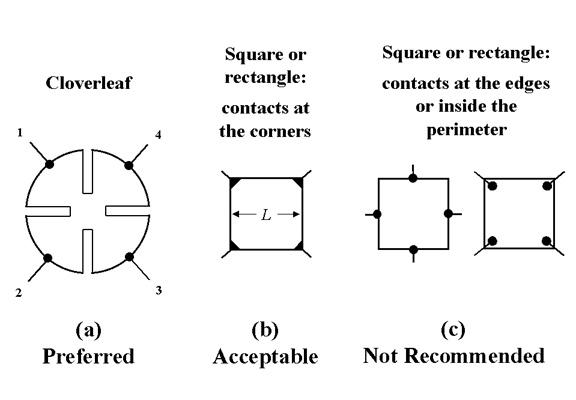
Figure 2. Examples of possible Van der Pauw configurations and their preference [12]
The objective of the resistivity measurement is to determine the sheet resistance RS. Van der Pauw demonstrated that there are actually two characteristic resistances RA and RB, associated with the corresponding terminals shown in Fig. 2. RA and RB are related to the sheet resistance RS through the van der Pauw equation
(3)
which can be solved numerically for RS.
The bulk electrical resistivity r can be calculated using
(4)
To obtain the two characteristic resistances, one applies a dc current I into contact 1 and out of contact 2 and measures the voltage V43 from contact 4 to contact 3. Next, one applies the current I into contact 2 and out of contact 3 while measuring the voltage V14 from contact 1 to contact 4 using a geometry shown in figure 3. RA and RB are calculated by means of the following expressions:
and
(5)
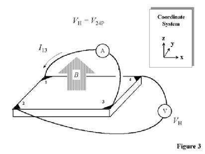
The objective of the Hall measurement in the Van der Pauw technique is to determine the sheet carrier density ns by measuring the Hall voltage VH. The Hall voltage measurement consists of a series of voltage measurements with a constant current I and a constant magnetic field B applied perpendicular to the plane of the sample. Conveniently, the same sample, shown again in Fig. 3, can also be used for the Hall measurement. To measure the Hall voltage VH, a current I is forced through the opposing pair of contacts 1 and 3 and the Hall voltage VH (= V24) is measured across the remaining pair of contacts 2 and 4. Once the Hall voltage VH is acquired, the sheet carrier density ns can be calculated via ns = IB/q|VH| from the known values of I, B, and q.
There are practical aspects which must be considered when carrying out Hall and resistivity measurements. Primary concerns are (1) ohmic contact quality and size, (2) sample uniformity and accurate thickness determination, (3) thermomagnetic effects due to nonuniform temperature, and (4) photoconductive and photovoltaic effects which can be minimized by measuring in a dark environment. Also, the sample lateral dimensions must be large compared to the size of the contacts and the sample thickness. Finally, one must accurately measure sample temperature, magnetic field intensity, electrical current, and voltage.
Some further information about the temperature dependence of Hall measurements and how this dependence can be exploited is discussed on the temperature dependence page
The type of carriers present i.e. n or p type is very important. There is a more detailed discussion on this area on the carrier type page
References
- http://www.eeel.nist.gov/812/effe.htm
- "Standard Test Methods for Measuring Resistivity and Hall Coefficient and Determining Hall Mobility in Single-Crystal Semiconductors," ASTM Designation F76, Annual Book of ASTM Standards, Vol. 10.05 (2000).
- E. H. Hall, "On a New Action of the Magnet on Electrical Current," Amer. J. Math. 2, 287-292 (1879).
- L. J. van der Pauw, "A Method of Measuring Specific Resistivity and Hall Effect of Discs of Arbitrary Shapes," Philips Res. Repts. 13, 1-9 (1958).
- L. J. van der Pauw, "A Method of Measuring the Resistivity and Hall Coefficient on Lamellae of Arbitrary Shape," Philips Tech. Rev. 20, 220-224 (1958).
- E. H. Putley, The Hall Effect and Related Phenomena, Butterworths, London (1960).
- D. C. Look, Electrical Characterization of GaAs Materials and Devices, John Wiley & Sons, Chichester (1989).
- D. K. Schroder, Semiconductor Material and Device Characterization, 2nd Edition, John Wiley & Sons, New York (1998).
- R. Chwang, B. J. Smith and C. R. Crowell, "Contact Size Effects on the van der Pauw Method for Resistivity and Hall Coefficient Measurement," Solid-State Electronics 17, 1217-1227 (1974).
- D. L. Rode, C. M. Wolfe and G. E. Stillman, "Magnetic-Field Dependence of the Hall Factor for Isotropic Media," J. Appl. Phys. 54, 10-13 (1983).
- D. L. Rode, "Low-Field Electron Transport," Semiconductors & Semimetals 10, 1-89 (1975).
- http://en.wikipedia.org/wiki/File:VanderPauwContactPlacement.jpg