
Scanning Tunnelling Microscopy / Scanning Tunnelling Spectroscopy
STM is an advanced type of computerised microscopy. The need for investigating features at much smaller dimensions than the wavelength of visible light led to invention of this instrument. STM operates differently to an optical microscope, looking at the electronic surface of a material, with a resolution of up to 2000 times the resolution available from an optical microscope.
The phenomena of quantum tunnelling allows for high resolution imaging of the surface, down to the scale of atomic separation (~0.3 nm), and has no counterpart in classical physics. Tunnelling probability is the probability that a particle can cross a barrier that classically it is forbidden from doing, to reach a lower final potential.
In the case of the STM, the reduction of separation between the sample and tip, of the order nanometres, electrons can tunnel through the classically forbidden region from one surface to another at lower potential.
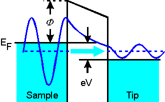
Illustration of the Fermi levels for a metallic surface and tip with the tip biased positive relative to the surface. At a positive tunneling voltage (eV) applied to the tip, the electrons from the occupied states in the valence band of the sample are caused to travel through the barrier to the unoccupied states of the tip. EF is the Fermi level of the sample, is the work function of the sample [1].
The blue arrow in the figure indicates electrons tunnelling from filled states in the sample into empty states in the tip according to:
The rapid decay of the current with distance z is due to the very small probability of tunneling across the vacuum barrier at large distances, with characteristic decay length relationship proportional to k-1, hence, the tunnel current depends exponentially on tip-surface separation.
The rapid decay of the current with separation z, leads to a high resolution in the z direction. Both tip and the sample must be conductive or semiconductive materials. When the separation is small enough, the electron wavefunctions overlap and by applying a bias voltage a tunnelling current is caused to flow.
The tunnelling current can be monitored in software, to utilise computer controlled feedback. This is used to keep the current at a constant level, by either changing the applied voltage, or the tip-sample separation of the system. This is possible due to the piezodrive construction, piezoelectric crystals expand or contract depending on the applied voltage, allowing tip/sample movement in x, y and z directions. The data is recorded and can be transformed into 2D / 3D topographic images of the local density of electronic states.
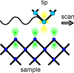
Microscopic view of STM imaging mechanism. An atomic state at the tip end, exemplified by a dz2 state protruding from the apex of a W tip, interacts with a two-dimensional array of atomic states, exemplified by sp3 states on Si surface. This results in a highly corrugated tunneling current distribution [1].
Setup Implementation Details
STM is a technique with susceptibility to interference. To obtain high quality images, sources of interference including electrical noise, external vibration, and thermal drift should be reduced to a minimum. Isolation of the instrument from the surrounding environment can help reduce the impact of interference on the signal received. To minimise vibrations it is possible to mount the system on pneumatic legs and/or the sample holder can be suspended on springs in a magnetic field. The effect of temperature variation can be minimised by a symmetrical design. STM can be performed in a variety of environments; air, inert gas, ultra high vacuum, liquid and electrolytes. The operating temperature ranges from very low temperatures of about 4K up to high temperatures of more than 1000K.
Imaging Modes
STM can be used in two important scanning modes; constant-height, and constant-current mode. In the constant-current mode the scanner is moved up and down, but the irregular surfaces can be measured with high precision, while the constant-height mode can provide useful information only for very smooth surfaces.
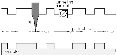
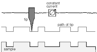
Diagrams to compare constant-height, and constant-current mode[2].
Constant-height mode represents a fast method for visualising surfaces, but provides reasonable data only for flat and smooth substrates. In the constant-height mode, the tip is held at constant height, set before the scan begins, and the tunnelling current is measured. The tunnelling current varies with the topographic and electronic characteristics of the sample.
Constant-current mode, although it takes longer to obtain images, is often preferred in experiments, as it offers precise detection and monitoring of irregular features of rough surfaces. The control system utilises a feedback loop to adjust the height, maintaining a constant tunnelling current. When an increase in the tunnelling current is registered at a value above the setpoint, the gap between tip and sample is automatically increased. If the tunnelling current is smaller, the tip is brought closer to the surface of the sample. Hence, the desired tunnelling current is maintained. The computer control system collates the signals and displays a two- or three-dimensional plot, generated from the tunnelling current or z piezo voltage measured at every point of the raster scan.
Scanning Tunnelling Spectroscopy (STS)
Scanning tunnelling spectroscopy is a technique used in scanning tunnelling microscopy to probe the local density of states and the gap of the investigated structure in order to obtain information about the conducting, semiconducting or insulating nature of the substrate. The goal in an STS experiment is to obtain the density of states of the sample. Because the spectroscopic information is acquired from both tip and sample the procedure requires a tip with a constant density of states or a free-electron metal tip. Assuming constant the density of states of the tip, the tunnelling current is evaluated by summing over all relevant states, where ρs represents the density of states of the sample, EF the energy at the Fermi level, eV the voltage applied to the tip and є energy parameter with finite value:
Differentiation dI/dV determines the energy dependence of density of states:
The STS procedure is applied by placing the tip over a specific spot on the sample. The feedback is shut off and the computer measures the tunnelling current variation as a function of voltage (or distance). The density of states can be determined by the modulation of the bias voltage. The spectroscopic curves can be acquired for single points, a regular pattern or for every raster point.
Return to electronic characterisation
References