
Reflection
Reflection or reflectivity measurments are usually to examine the layer thickness of insulating layer on semiconducting substrates and epitaxial semiconductor films. The reflectance R of the structure( absorbing layer of thickness d1 on a nonabsorbing ) as show in Fig. 1(a) is given by
---------(1)
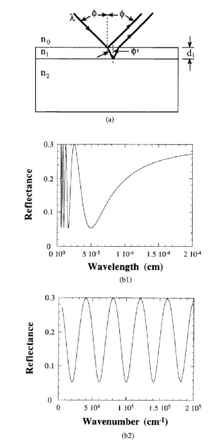
Fig.1 (a) Reflection spectroscopy schematic; (b) theoretical reflectance for SiO2 on Si.
Tox= 100 mm, n0 = 1, n1= 1.46, and n2= 3.42,
Where ;
;
;
For a nonabsorbing layer, in Eq.(1)
The reflectance exhibits maxima at the wavelengths (max)
---------(2)
Where m = 1,2,3,…
Taking Eq.(2) at two maxima and subtracting one from the other can give the layer thickness d1
---------(3)
Where i= number of complete cycles from to
, the two wavelength peaks that bracket the i cycles. For example in Fig. 1(b2) for the first two peaks, i= 1,
= 1.62x105cm-1
and =1.22x105cm-1 or i= 3,
= 1.62x105cm-1 and
= 4.2x104cm-1 is obtained a similar thickness.
[Ref.] D.K. Schroder,Semiconductor material and device characterization, 2nd edition,John Wiley & Son,1998.