
Electron Diffraction
Electron Diffraction
The wave-particle duality of nature results in particles having both wave-like and particle-like properties. The wave-like properties of objects means that we can perform diffraction using them, as with X-ray photons. However, this time we extend from massless particles to those with mass, including the electron and the neutron.
In this case, the wavelength of an electron is given by the de Broglie relation, as shown in Equation (1)
(1)
where h is Planck's constant and p is the electron momentum. As the momentum is related to the velocity and, in turn, the velocity is dependent upon the accelerating force i.e. an electric potential we see that Equation (1) can be written
where is the mass of the electron and U is the electric potential through which the electron is accelerated. Note that relativistic effects are ignored here.
As both LEED and RHEED are surface sensitive techniques note that the Ewald spherechanges. For a bulk structure, which has periodicity in three dimensions the solutions to the Ewald sphere result in spots. However, the loss of periodicity in one dimension, perpendicular to the plane of the surface, causes these spots to elongate into infinitely long rods that extend outwards from the surface as illustrated in Figure (1). The techniques described below, LEED and RHEED, both view the Ewald sphere in subtly different ways.
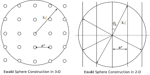 |
| Figure (1): The Ewald sphere in both two- and three-dimensions showing the change in reciprocal lattice points to rods. The dashed horizontal line on the 2-D plot represents the surface, electron paths above this are back-scattered. Correspondingly, below the line represents forward-scattering into the crystal. a* is the reciprocal lattice vector and ki is the incident electron wavevector, θD is the diffraction angle. |
LEED (Low Energy Electron Diffraction)
In LEED the electrons used have energies in the range of 20 to 100 eV. At 20 eV these electrons have mean free paths of approximately 5 Å and wavelengths of around 3 Å [1]. The surface of a crystal is typically only 10 Å thick, with a lattice parameter of approximately 5 Å and so the electrons are well suited for the study of surfaces.
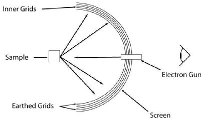 |
| Figure (2): Schematic of a typical LEED optics set-up |
The typical layout of LEED optics, set to operate as a retarding field analyser (RFA), is illustrated in Figure (2). Electrons back-scattered from the surface travel towards a series of grids. The inner grid, closest to the sample, is held at ground and screens the potentials of the outer grids. The central grids are held at the same potential as the electron gun, VE but features an offset δV, which is typically of the order 10 V. This potential filters out electrons who have an energy lower than eVE, the incident electron energy. Another earthed grid filters out the large potential of the screen, which is held at +5 kV and accelerates electrons towards a fluorescent screen. The large screen potential provides scattered electrons with a large enough kinetic energy, so that a LEED pattern will be produced. The diffraction pattern then seen is a magnified version of the surface reciprocal lattice.
Due to the geometry of this arrangement the incident electron wavevector effectively looks 'down' on the Ewald sphere and views the infinitely long rods as spots, giving rise to the characteristic spot patterns seen. A side-effect of the extension of lattice points into rods is that as the incident electron energy is varied spots do not go extinct but instead move. This provides a useful tool in the determination of surface structure and atomic positions. By studying the intensity of a spot and it location over a range of energies, then the position of atoms on the surface can be studied due to their effect on the scattered electrons. This is known as LEED I-V.
The energy distribution of emitted electrons is shown in Figure (3).
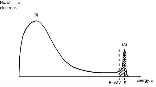 |
| Figure (3): Energy distribution of back-scattered electrons in LEED, reproduced from (2). |
Peak (A), centred around the incident electron energy E, is the elastically back-scattered peak and is of interest in LEED studies whereas peak (B) is the secondary electron peak which arises from inelastically scattered electrons and is not of interest. Through the introduction of the offset voltage, δV, any electrons with an energy equal to or lower than are filtered out and are not detected.
RHEED (Reflection High-Energy Electron Diffraction)
In RHEED electrons of between 8 and 20 keV impinge upon a surface at angles of approximately 1o - 3o. A typical RHEED set-up consists of an electron gun, sample and a phosphor screen and a typical geometry is illustrated on the MBE page. Using this geometry, RHEED provides the unique ability to monitor growth on a surface in real-time whilst the grazing incidence of the electron beam ensures surface specificity.
In RHEED the electron beam 'slices' through the reciprocal lattice rods, giving RHEED patterns a unique streaky pattern. Due to variations in the energy and angular divergence of the incident electron beam, the rods gain a finite width. As the electron beam intersects these rods they form streaks. The shape of the RHEED pattern observed provides a variety of information regarding the periodicity and structure of the surface. A 'spotty' pattern may be the result of transmission electron diffraction through 3D islands, with angled streaks indicating a faceted surface. Oscillations in the pattern intensity can be used to obtain the growth rate of layers during Frank-van der Merwe growth. As each monolayer completes the intensity of streak increases towards its maximum, representing the ordered nature of the complete layer. The period of this oscillation is representative of the time taken to complete each layer and from this a growth rate can be deduced.
SAED (Selected Area Electron Diffraction)
Due to the high energy electrons used in TEM, often of the order picometres, we can also use TEM as a diffraction imaging technique. The tightly focused electron beam used in TEM allows for diffraction of smaller crystal grains and is useful in the study of poly-crystalline material, enabling the characterisation of multiple crystallographically orientated micro-crystals. As with TEM the sample must be electron transparent, i.e. sufficiently thin for electrons to pass through, however, the sample does not necessarily need to be crystalline. Amorphous samples can also provide a diffuse diffraction pattern, as can polycrystalline materials (over larger areas). By combining standard imaging and SAED, TEM can be used to study the crystal nature of a material in great detail.
References
- G. Attard and C. Barnes (2003), Surfaces, Oxford University Press
- D. P. Woodruff and T. Delchar (1994), Modern Techniques of Surface Science, Cambridge University Press
Bibliography
- A. Ichimiya and P. I. Cohen (2004), Reflection High Energy Electron Diffraction, Cambridge University Press, ISBN 0-521-45373-9