
Facilities
Semiconductor Device Fabrication Laboratory
The Semiconductor Device Fabrication Laboratory is operated as part of the Science City Research Alliance between the University of Warwick and the University of Birmingham. The cleanroom facility's key users are the Quantum Devices group, the Power Electronics Applications and Technology in Energy Research (PEATER) group and the Nano-Silicon group. The facility is a state-of-the-art Class 1000 cleanroom with an extensive suite of processing and testing tools, including lithography, etching, deposition, annealing, microscopic inspection and physical, optical and electrical measurements. More information about the cleanroom facility can be found here.
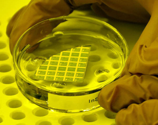
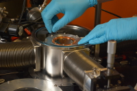
Sample in developer solution
Collaboration
PEATER and School of Engineering
The cleanroom fabrication laboratory is shared between the Quantum Devices group and the PEATER group. The PEATER group uses the facility to study silicon carbide, with the two groups benefiting from each other’s experience and expertise in fabrication and characterisation techniques. In addition, the Quantum Devices group makes use of other expertise in the School of Engineering, including the Microscopy and Analysis Laboratory. More information is available about the PEATER group and research in the School of Engineering.
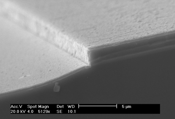
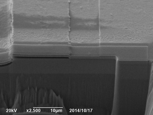
Deposited metal viewed by scanning electron microscope
Nano-Silicon Group
The Quantum Devices and PEATER groups frequently collaborate with the Nano-Silicon group in the Department of Physics. The Nano-Silicon group has expertise in material and device characterisation and group IV material growth, complementing the fabrication expertise and facilities in Engineering. The Quantum Devices group makes use of the Nano-Silicon group’s low-temperature characterisation tools and the groups are collaborating to explore the prospects of growing Si-Ge-InSb layer structures to improve compatibility between InSb and mainstream fabrication techniques. More information is available about the Nano-Silicon group and research in the Department of Physics.
PhD students from Nano-Si and Quantum Devices performing low-temperature characterisation
Surface, Interface and Thin Film Group
The Surface, Interface and Thin Film group in the Department of Physics offers significant resources and expertise to the Quantum Devices group. The Surface, Interface and Thin Film group specialises in surface science and, as such, offers techniques such as X-ray Photoelectron Spectrometry (XPS), Hall effect measurements and Fourier Transform Infrared (FTIR) Spectroscopy. The Surface, Interface and Thin Film group also has some experience with III-V materials (such as InN) and the two groups benefit from each other’s contrasting expertise. More information is available about the Surface, Interface and Thin Film group and research in the Department of Physics.
Sample being analysed by X-ray photoelectron spectrometry (XPS)
Microscopy Group
The University of Warwick houses a state-of-the-art microscopy facility, equipped with an extensive suite of techniques such as atomic force microscopy (AFM), scanning electron microscopy (SEM) and transmission electron microscopy (TEM). The facility is available to groups throughout the university and the Quantum Devices group uses the facility for physical and compositional analysis using SEM, as well as making use of the microscopy group’s expertise in AFM and TEM. More information is available about the Microscopy group and research in the Department of Physics.
Cross-section view created using focused ion beam (FIB) cut and scanning electron microscope (SEM)
Tim Jones Group and Department of Chemistry
The III-V molecular beam epitaxy (MBE) facility in the Department of Chemistry is jointly operated by the Tim Jones group and the Quantum Devices group. The MBE facility is operated by Mark Ashwin and is used both as a material source for device experiments and for growth science experiments, such as dilute bismide and nitride materials. The Tim Jones group also provides access to an atomic force microscope (AFM), used by the Quantum Devices group for materials characterisation. More information is available about the Tim Jones group and research in the Department of Chemistry.
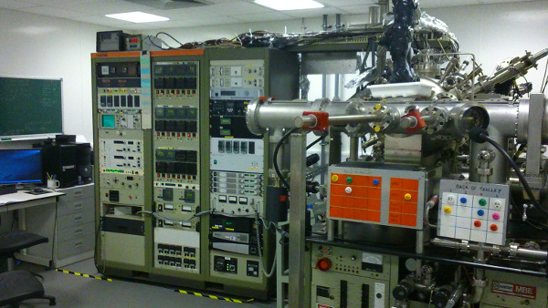
Control systems and vacuum chambers in the MBE lab
University of Liverpool – Functional Materials Research Group
The Quantum Devices group is engaged in collaborative work with the atomic layer deposition (ALD) facility at the University of Liverpool. ALD processing is provided by Professor Paul Chalker’s team in the Functional Materials group, a group which is part of the School of Engineering’s Centre for Materials and Structures. The ALD capability is used for investigating material interfaces, with the results collected at Warwick being fed back to the group at Liverpool to aid process development. More information is available about the Centre for Materials and Structures, Paul Chalker and research at the University of Liverpool’s School of Engineering.
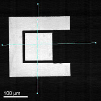
Markers for aligning process steps
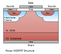
Structure of high-power MOSFET used by the PEATER group
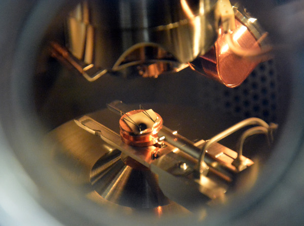
Low-temperature probe station vacuum chamber being loaded
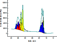
Spectra acquired by XPS
A device is prepared for electron beam-induced current (EBIC) experiment
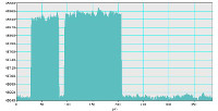
Results of the EBIC experiment
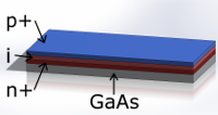
Illustration of different layers grown by MBE