Ultrafast optical techniques provide powerful probes of different states of matter, using light pulses that have femtosecond duration. In Warwick our activities span a number of areas:
studying the dynamics of the light-matter interaction in novel compounds and nanomaterials via terahertz spectroscopy and pump-probe methods,
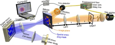
performing terahertz medical imaging and spectroscopy,
developing methods and components for terahertz imaging and terahertz spectroscopy.
Group facilities
The Group has labs across the campus, in the main Physics building, Materials and Analytical Sciences, and Millburn House. Read more about our experimental capabilities in terahertz science and technology. We also run the Warwick Centre for Ultrafast Spectroscopy Research Technology Platform.
Please get in touch if you are interested in a PhD or MSc by Research in the group. We are also happy to support postdoctoral researchers to apply for fellowship schemes.
We use pump/probe spectroscopy to study how light and matter interact on femtosecond to nanosecond timescales. Using visible probes we can track electronic processes, while infrared radiation lets us study vibrational states of molecules and atomic-scale defects in semiconductors.
Performing in vivo studies of the THz properties of skin is a major initiative in the group, supported by the EPSRC Terabotics Programme GrantLink opens in a new window. We develop robust measurement protocols and test them on a statistically significant number of patients, cross-checking with other methods.
A major strand of our research is to improve our knowledge of the fundamental science underpinning new semiconductor materials, such as metal-halide perovskites, which are often attractive for photovoltaic applications.
We develop new THz devices and integrate them into novel systems designs that can perform THz imaging and THz spectroscopy faster, and with increased capabilities (e.g. polarisation control; robot-controlled probes).
BFM Healy, SL Pain, J. Lloyd-Hughes, NE Grant and JD Murphy Materials Research Express 11 015002 (Jan 2024)
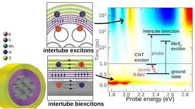
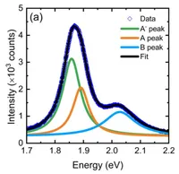
Monolayer molybdenum disulfide (MoS2) is a promising candidate for inclusion in optoelectronic technologies, owing to its two-dimensional (2D) nature and resultant novel photoluminescence (PL). Chemical vapour deposition (CVD) is an important method for the preparation of large-area films of monolayer MoS2. The PL character of as-prepared monolayer MoS2 must be well understood to facilitate detailed evaluation of any process-induced effects during device fabrication. We comparatively explore the PL emission from four different commercially available CVD-grown MoS2 monolayer films. We characterize the samples via Raman and PL spectroscopy, using both single-spot and mapping techniques, while atomic force microscopy (AFM) is applied to map the surface structure. Via multipeak fitting, we decompose the PL spectra into constituent exciton and trion contributions, enabling an assessment of the quality of the MoS2 monolayers. We find that the PL character varies significantly from sample to sample. We also reveal substantial inhomogeneity of the PL signal across each individual MoS2 film. We attribute the PL variation to non-uniform MoS2 film morphologies that result from the nucleation and coalescence processes during the CVD film development. Understanding the large variability in starting PL behaviour is vital to optimize the optoelectronic properties for MoS2-based devices.
T.J. Keat, D. J. L. Coxon, R.J. Cruddace, V. G. Stavros, M. E. Newton, and J. Lloyd-Hughes Diamond and Related Materials 141110661 (Jan 2024)
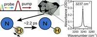
The dynamics of the 3237 cm−1 local vibrational mode in diamond, associated with an unknown defect, was investigated using ultrafast infrared pump-probe spectroscopy. When pumped at 3237 cm−1, a degenerate probe was used to study the ground state's recovery, while a non-degenerate probe tracked excited state absorption at 3029 cm−1, corresponding to the 1 → 2 vibrational state transition. The similar population lifetimes for the ground state recovery and excited state absorption suggests a single population decay pathway, with a lifetime of T1=2.2+-0.1ps. Perturbed free induction decay signals observed in negative time delays gave the dephasing time of the coherent state between the 0 and 1 vibrational states, and further predicted the 3029 cm−1 transition. Images from FTIR microscopy show that the 3237 cm−1 feature and the 3107 cm−1 absorption line from the N3VH0 defect are not correlated, and our pump-probe study shows the 3237 cm−1 feature does not share a common ground state with the N3VH0 defect, both of which suggest that this local vibrational mode does not originate from the N3VH0 defect. A calibration factor was obtained via a Morse potential model constrained by the observed transition energies, which relates the concentration of the defect producing the 3237 cm−1 feature to its absorption coefficient measured by FTIR spectroscopy. Based on FTIR absorption spectroscopy under uniaxial stress, we further assign a trigonal symmetry character to the defect that gives the 3237 cm−1 feature. The results presented are consistent with the theory that the 3237 cm−1 feature originates from the N4VH defect, the quantification of which allows better tracking of the nitrogen content in diamond.
A. Ren, H. Wang, L. Dai, J. Xia, E. Butler-Caddle, J.A. Smith, ... S.A. Hindmarsh, A.M. Sanchez, J. Lloyd-Hughes, S. J Sweeney, ... and Wei Zhang Nature Photonics17, 798–805 (July 2023)
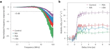
Light-emitting diodes (LEDs) are ubiquitous in modern society, with applications spanning from lighting and displays to medical diagnostics and data communications. Metal-halide perovskites are promising materials for LEDs because of their excellent optoelectronic properties and solution processability. Although research has progressed substantially in optimizing their external quantum efficiency, the modulation characteristics of perovskite LEDs remain unclear. Here we report a holistic approach for realizing fast perovskite photonic sources on silicon based on tailoring alkylammonium cations in perovskite systems. We reveal the recombination behaviour of charged species at various carrier density regimes relevant for their modulation performance. By integrating a Fabry–Pérot microcavity on silicon, we demonstrate perovskite devices with efficient light outcoupling. We achieve device modulation bandwidths of up to 42.6 MHz and data rates above 50 Mbps, with further analysis suggesting that the bandwidth may exceed gigahertz levels. The principles developed here will support the development of perovskite light sources for next-generation data-communication architectures. The demonstration of solution-processed perovskite emitters on silicon substrates also opens up the possibility of integration with micro-electronics platforms.
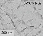
M.G. Burdanova, A.P. Tsapenko, S. Ahmad, E.I. Kauppinen and J. Lloyd-Hughes Nanotechnology 34405203, (June 2023)
Mixed-nanomaterial composites can combine the excellent properties of well-known low-dimensional nanomaterials. Here we highlight the potential of one-dimensional single-walled carbon nanotubes interfaced with two-dimensional graphene by exploring the composite's ac conductivity and photoconductivity, and the influence of HAuCl4 doping. In the composite, the equilibrium terahertz conductivity from free carrier motion was boosted, while the localised plasmon peak shifted towards higher frequencies, which we attribute to shorter conductivity pathways in the composite. A negative terahertz photoconductivity was observed for all samples under 410nm optical excitation and was reproduced by a simple model, where the Drude spectral weight and the momentum scattering rate were both lowered under photoexcitation. The composite had an enhanced modulation depth in comparison to reference carbon nanotube films, while retaining their characteristically fast (picosecond) response time. The results show that CNT-graphene composites offer new opportunities in devices by controlling charge carrier transport and tuning their optoelectronic properties.