Ultrafast & Terahertz Photonics Group
|
Ultrafast optical techniques provide powerful probes of different states of matter, using light pulses that have femtosecond duration. In Warwick our activities span a number of areas:
|
Group facilitiesThe Group has labs across the campus, in the main Physics building, Materials and Analytical Sciences, and Millburn House. Read more about our experimental capabilities in terahertz science and technology. We also run the Warwick Centre for Ultrafast Spectroscopy Research Technology Platform. 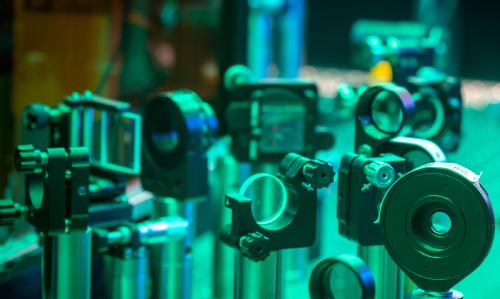
We make use of a wide range of Warwick's excellent materials analysis equipment, including X-ray diffraction, Raman spectroscopy, electron microscopy and magnetometry. |
Join the group!We have funded PhD positions available to work on nanoscale imaging of perovskitesLink opens in a new window, coherent vibrations of defect in diamond, Link opens in a new window THz sensing for biomedical applicationsLink opens in a new window and ultrafast studies of battery materialsLink opens in a new window. These are available for UK students and potentially for exceptional international students. Please get in touch if you are interested in PhD or MSc by Research topics in the group. We also support postdoctoral researchers to apply for independent fellowship schemes - let us know if that appeals. 
Group, Theses & PhotosContact details for our current group members and our photo gallery. For recent theses from the group, please see here. |
Research areas
Nanomaterials
We use pump/probe spectroscopy to study how light and matter interact on femtosecond to nanosecond timescales. Using visible probes we can track electronic processes, while infrared radiation lets us study vibrational states of molecules and atomic-scale defects in semiconductors.
Recent papers:
Untangling free carrier and exciton dynamics in layered hybrid perovskites using ultrafast optical and terahertz spectroscopy
Quantifying photoluminescence variability in monolayer molybdenum disulfide films grown by chemical vapour deposition
Terahertz medical imaging
Performing in vivo studies of the THz properties of skin is a major initiative in the group, supported by the EPSRC Terabotics Programme GrantLink opens in a new window. We develop robust measurement protocols and test them on a statistically significant number of patients, cross-checking with other methods.
Recent papers:
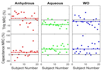
Effect of transdermal drug delivery patches on the stratum corneum: in vivo inspection with a handheld terahertz probe
Terahertz probe for real time in vivo skin hydration evaluation
Spectroscopic insight on impact of environment on natural photoprotectants
Semiconductors and Energy materials
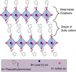
A major strand of our research is to improve our knowledge of the fundamental science underpinning new semiconductor materials, such as metal-halide perovskites, which are often attractive for photovoltaic applications.
Recent papers:
Distinguishing carrier transport and interfacial recombination at perovskite/transport-layer interfaces using ultrafast spectroscopy and numerical simulation
Temperature-Dependent Structural and Optoelectronic Properties of the Layered Perovskite 2-Thiophenemethylammonium Lead Iodide
Untangling free carrier and exciton dynamics in layered hybrid perovskites using ultrafast optical and terahertz spectroscopy
Terahertz components, methods and techniques
We develop new THz devices and integrate them into novel systems designs that can perform THz imaging and THz spectroscopy faster, and with increased capabilities (e.g. polarisation control; robot-controlled probes).
Recent papers:
Dual-Beam THz Spectrometer with Low-Aberration Optics and Off-Axis Multipixel Photoconductive Emitters for Reduced Systematic Errors
Simultaneous measurement of orthogonal terahertz fields via an emission multiplexing scheme
Optimum Optical Designs for Diffraction-Limited Terahertz Spectroscopy and Imaging Systems Using Off-Axis Parabolic Mirrors
Recent publication highlights [filter by topic: view all | highlights | THz | perovskites | nano | biomedical]
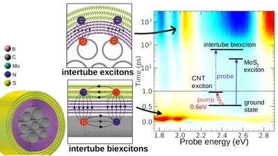
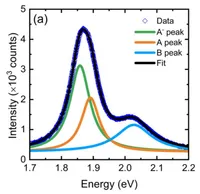
Tunable Photoluminescence from Monolayer Molybdenum Disulfide
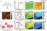
BFM Healy, SL Pain, J. Lloyd-Hughes, NE Grant and JD Murphy
Adv. Mater. Interfaces 11 2400305 (Jul 2024)
Untangling free carrier and exciton dynamics in layered hybrid perovskites using ultrafast optical and terahertz spectroscopy
Folusho Helen Balogun, Nathaniel P Gallop, Dumitru Sirbu, Jake D Hutchinson, Nathan Hill, Jack M Woolley, David Walker, Stephen York, Pablo Docampo and Rebecca L Milot
Mater. Res. Express 11 025503 (Feb 2024)
Quantifying photoluminescence variability in monolayer molybdenum disulfide films grown by chemical vapour deposition
BFM Healy, SL Pain, J. Lloyd-Hughes, NE Grant and JD Murphy
Materials Research Express 11 015002 (Jan 2024)
The 3237 cm−1 diamond defect: Ultrafast vibrational dynamics, concentration calibration, and relationship to the N3VH0 defect
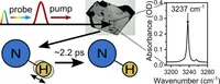
T.J. Keat, D. J. L. Coxon, R.J. Cruddace, V. G. Stavros, M. E. Newton, and J. Lloyd-Hughes
Diamond and Related Materials 141 110661 (Jan 2024)