Ultrafast optical techniques provide powerful probes of different states of matter, using light pulses that have femtosecond duration. In Warwick our activities span a number of areas:
studying the dynamics of the light-matter interaction in novel compounds and nanomaterials via terahertz spectroscopy and pump-probe methods,
performing terahertz medical imaging and spectroscopy,
developing methods and components for terahertz imaging and terahertz spectroscopy.
Group facilities
The Group has labs across the campus, in the main Physics building, Materials and Analytical Sciences, and Millburn House. Read more about our experimental capabilities in terahertz science and technology. We also run the Warwick Centre for Ultrafast Spectroscopy Research Technology Platform.
Please get in touch if you are interested in a PhD or MSc by Research in the group. We are also happy to support postdoctoral researchers to apply for fellowship schemes.
We use pump/probe spectroscopy to study how light and matter interact on femtosecond to nanosecond timescales. Using visible probes we can track electronic processes, while infrared radiation lets us study vibrational states of molecules and atomic-scale defects in semiconductors.
Performing in vivo studies of the THz properties of skin is a major initiative in the group, supported by the EPSRC Terabotics Programme GrantLink opens in a new window. We develop robust measurement protocols and test them on a statistically significant number of patients, cross-checking with other methods.
A major strand of our research is to improve our knowledge of the fundamental science underpinning new semiconductor materials, such as metal-halide perovskites, which are often attractive for photovoltaic applications.
We develop new THz devices and integrate them into novel systems designs that can perform THz imaging and THz spectroscopy faster, and with increased capabilities (e.g. polarisation control; robot-controlled probes).
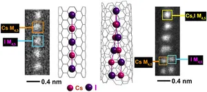
R.J. Kashtiban, M.G. Burdanova, A. Vasylenko, J. Wynn, P.V.C. Medeiros, Q. Ramasse, A.J. Morris, D. Quigley, J. Lloyd-Hughes and J. Sloan
ACS Nano 1513389 (Aug 2021)
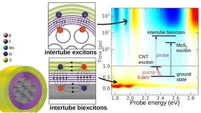
One-dimensional (1D) atomic chains of CsI were previously reported in double-walled carbon nanotubes with ∼0.8 nm inner diameter. Here, we demonstrate that, while 1D CsI chains form within narrow ∼0.73 nm diameter single-walled carbon nanotubes (SWCNTs), wider SWCNT tubules (∼0.8–1.1 nm) promote the formation of helical chains of CsI 2 × 1 atoms in cross-section. These CsI helices create complementary oval distortions in encapsulating SWCNTs with highly strained helices formed from strained Cs2I2 parallelogram units in narrow tubes to lower strain Cs2I2 units in wider tubes. The observed structural changes and charge distribution were analyzed by density-functional theory and Bader analysis. CsI chains also produce conformation-selective changes to the electronic structure and optical properties of the encapsulating tubules. The observed defects are an interesting variation from defects commonly observed in alkali halides as these are normally associated with the Schottky and Frenkel type. The energetics of CsI 2 × 1 helix formation in SWCNTs suggests how these could be controllably formed.
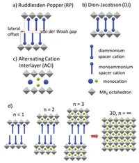
D. Sirbu, F. H. Balogun, R. L. Milot and P. Docampo
Advanced Energy Materials (May 2021)
Layered hybrid perovskites (LPKs) have emerged as a viable solution to address perovskite stability concerns and enable their implementation in wide-scale energy harvesting. Yet, although more stable, the performance of devices incorporating LPKs still lags behind that of state-of-the-art, multi-cation perovskite materials. This is typically assigned to their poor charge transport, currently caused by the choice of cations used within the organic layer. On balance, a compromise between efficiency and stability is sought, involving careful control of phase purity and distribution, interfaces and energy/charge transfer processes. Further progress is hindered by the difficulty in identifying the fundamental optoelectronic processes in these materials. Here, the high exciton binding energy of LPKs lead to the formation of multiple photoexcited species, which greatly complicate measurement interpretation. In this light, this review gives an overview of how complementary measurement techniques must be used to separate the contributions from the different species in order to identify device bottlenecks, and become a useful tool to narrow down the limitless list of organic cations. A move away from making compromises to mitigate the impact of poor charge transport is required. The root of the problem must be addressed instead through rational design of the interlayer cations.
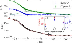
M. Monti, K.D.G.I. Jayawardena, E. Butler-Caddle, R.M.I. Bandara, J.M. Woolley, M. Staniforth, S.R.P. Silva and J. Lloyd-Hughes
Phys. Rev. B 102 245204 (Dec 2020) [ pdf ] [ ref ]
The electron-phonon interaction controls the intrinsic mobility of charges in metal halide perovskites, and determines the rate at which carriers lose energy. Here, the carrier mobility and cooling dynamics were directly examined using a combination of ultrafast transient absorption spectroscopy and optical pump, THz probe spectroscopy, in perovskites with different lead and tin content, and for a range of carrier densities. Significantly, the carrier mobility in the “hot phonon bottleneck” regime, where the LO phonon bath keeps carriers warm, was found to be similar to the mobility of cold carriers. A model was developed that provides a quantitative description of the experimental carrier cooling dynamics, including electron-phonon coupling, phonon-phonon coupling and the Auger mechanism. In the Pb and Sn alloy the duration of the hot carrier regime was extended as a result of the slower decay of optical phonons. The findings offer an intuitive link between macroscopic properties and the underlying microscopic energy transfer processes, and suggest new routes to control the carrier cooling process in metal halide perovskites to optimize optoelectronic devices.
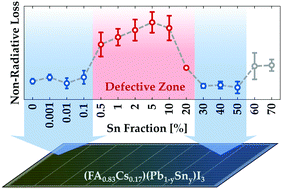
M. T. Klug, R. L. Milot, J.B. Patel, T. Green, H. C. Sansom, M. D. Farrar, A. J. Ramadan, S. Martani, Z. Wang, B. Wenger, J. M. Ball, L. Langshaw, A. Petrozza, M. B. Johnston, L. M. Herz and H. J. Snaith
Energy & Environmental Science (May 2020)
Current designs for all-perovskite multi-junction solar cells require mixed-metal Pb–Sn compositions to achieve narrower band gaps than are possible with their neat Pb counterparts. The lower band gap range achievable with mixed-metal Pb–Sn perovskites also encompasses the 1.3 to 1.4 eV range that is theoretically ideal for maximising the efficiency of single-junction devices. Here we examine the optoelectronic quality and photovoltaic performance of the ((HC(NH2)2)0.83Cs0.17)(Pb1−ySny)I3 family of perovskite materials across the full range of achievable band gaps by substituting between 0.001% and 70% of the Pb content with Sn. We reveal that a compositional range of “defectiveness” exists when Sn comprises between 0.5% and 20% of the metal content, but that the optoelectronic quality is restored for Sn content between 30–50%. When only 1% of Pb content is replaced by Sn, we find that photoconductivity, photoluminescence lifetime, and photoluminescence quantum efficiency are reduced by at least an order of magnitude, which reveals that a small concentration of Sn incorporation produces trap sites that promote non-radiative recombination in the material and limit photovoltaic performance. While these observations suggest that band gaps between 1.35 and 1.5 eV are unlikely to be useful for optoelectronic applications without countermeasures to improve material quality, highly efficient narrower band gap absorber materials are possible at or below 1.33 eV. Through optimising single-junction photovoltaic devices with Sn compositions of 30% and 50%, we respectively demonstrate a 17.6% efficient solar cell with an ideal single-junction band gap of 1.33 eV and an 18.1% efficient low band gap device suitable for the bottom absorber in all-perovskite multi-junction cells.