
Ultrafast & Terahertz Photonics Group
|
Ultrafast optical techniques provide powerful probes of different states of matter, using light pulses that have femtosecond duration. In Warwick our activities span a number of areas:
|
Group facilitiesThe Group has labs across the campus, in the main Physics building, Materials and Analytical Sciences, and Millburn House. Read more about our experimental capabilities in terahertz science and technology. We also run the Warwick Centre for Ultrafast Spectroscopy Research Technology Platform. 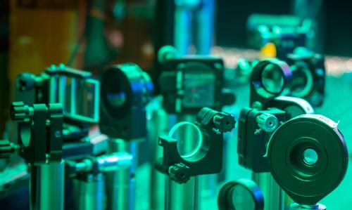
We make use of a wide range of Warwick's excellent materials analysis equipment, including X-ray diffraction, Raman spectroscopy, electron microscopy and magnetometry. |
Join the group!Please get in touch if you are interested in a PhD or MSc by Research in the group. We are also happy to support postdoctoral researchers to apply for fellowship schemes. 
Group, Theses & PhotosContact details for our current group members and our photo gallery. For recent theses from the group, please see here. |
Research areas
Nanomaterials
We use pump/probe spectroscopy to study how light and matter interact on femtosecond to nanosecond timescales. Using visible probes we can track electronic processes, while infrared radiation lets us study vibrational states of molecules and atomic-scale defects in semiconductors.
Recent papers:
Quantifying photoluminescence variability in monolayer molybdenum disulfide films grown by chemical vapour deposition
The 3237 cm−1 diamond defect: Ultrafast vibrational dynamics, concentration calibration, and relationship to the N3VH0 defect
Terahertz medical imaging
Performing in vivo studies of the THz properties of skin is a major initiative in the group, supported by the EPSRC Terabotics Programme GrantLink opens in a new window. We develop robust measurement protocols and test them on a statistically significant number of patients, cross-checking with other methods.
Recent papers:
Terahertz probe for real time in vivo skin hydration evaluation
Spectroscopic insight on impact of environment on natural photoprotectants
The 2023 terahertz science and technology roadmap
Semiconductors and Energy materials
A major strand of our research is to improve our knowledge of the fundamental science underpinning new semiconductor materials, such as metal-halide perovskites, which are often attractive for photovoltaic applications.
Recent papers:
Terahertz Emission via Optical Rectification in a Metal-Free Perovskite Crystal
High-bandwidth perovskite photonic sources on silicon
Resolving the Ultrafast Charge Carrier Dynamics of 2D and 3D Domains within a Mixed 2D/3D Lead-Tin Perovskite
Terahertz components, methods and techniques
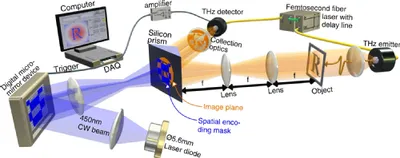
We develop new THz devices and integrate them into novel systems designs that can perform THz imaging and THz spectroscopy faster, and with increased capabilities (e.g. polarisation control; robot-controlled probes).
Recent papers:
Simultaneous measurement of orthogonal terahertz fields via an emission multiplexing scheme
Optimum Optical Designs for Diffraction-Limited Terahertz Spectroscopy and Imaging Systems Using Off-Axis Parabolic Mirrors
The 2023 terahertz science and technology roadmap
Recent publication highlights [filter by topic: view all | highlights | THz | perovskites | nano | biomedical]
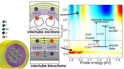
Ultrafast Optoelectronic Processes in 1D Radial van der Waals Heterostructures: Carbon, Boron Nitride, and MoS2 Nanotubes with Coexisting Excitons and Highly Mobile Charges
M.G. Burdanova, R.J. Kashtiban, Y. Zheng, R. Xiang, S. Chiashi, J.M. Woolley, M. Staniforth, E. Sakamoto-Rablah, X. Xie, M. Broome, J. Sloan, A. Anisimov, E.I. Kauppinen, S. Maruyama and J. Lloyd-Hughes
Nano Lett. 20 5, 3560 (Apr 2020) [ free e-print ] [ preprint pdf ] [ ref ]
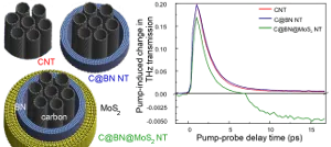 Heterostructures built from 2D, atomically thin crystals are bound by the van der Waals force and exhibit unique optoelectronic properties. Here, we report the structure, composition and optoelectronic properties of 1D van der Waals heterostructures comprising carbon nanotubes wrapped by atomically thin nanotubes of boron nitride and molybdenum disulfide (MoS2). The high quality of the composite was directly made evident on the atomic scale by transmission electron microscopy, and on the macroscopic scale by a study of the heterostructure’s equilibrium and ultrafast optoelectronics. Ultrafast pump–probe spectroscopy across the visible and terahertz frequency ranges identified that, in the MoS2 nanotubes, excitons coexisted with a prominent population of free charges. The electron mobility was comparable to that found in high-quality atomically thin crystals. The high mobility of the MoS2 nanotubes highlights the potential of 1D van der Waals heterostructures for nanoscale optoelectronic devices.
Approaching the Shockley-Queisser limit for fill factors in lead–tin mixed perovskite photovoltaics
K.D.G.I. Jayawardena, R.M.I. Bandara, M. Monti, E. Butler-Caddle, T. Pichler, H. Shiozawa, Z. Wang, S. Jenatsch, S.J. Hinder, M.G. Masteghin, M. Patel, H.M. Thirimanne, W. Zhang, R.A. Sporea, J. Lloyd-Hughes and S. R. P. Silva
J. Mater. Chem. A 8 693 (Jan 2020) [ pdf ] [ ref ]
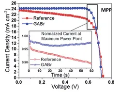 The performance of all solar cells is dictated by charge recombination. A closer to ideal recombination dynamics results in improved performances, with fill factors approaching the limits based on Shockley-Queisser analysis. It is well known that for emerging solar materials such as perovskites, there are several challenges that need to be overcome to achieve high fill factors, particularly for large area lead-tin mixed perovskite solar cells. Here we demonstrate a strategy towards achieving fill factors above 80% through post-treatment of a lead-tin mixed perovskite absorber with guanidinium bromide for devices with an active area of 0.43 cm2. This bromide post-treatment results in a more favourable band alignment at the anode and cathode interfaces, enabling better bipolar extraction. The resulting devices demonstrate an exceptional fill factor of 83%, approaching the Shockley–Queisser limit, resulting in a power conversion efficiency of 14.4% for large area devices.
The Effects of Doping Density and Temperature on the Optoelectronic Properties of Formamidinium Tin Triiodide Thin Films
R. L. Milot, M. T. Klug, C. L. Davies, Z. Wang, H. Kraus, H. J. Snaith, M. B. Johnston, and L. M. Herz
Advanced Materials (Sept 2018) [ pdf ] [ ref ]
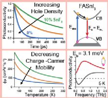 Optoelectronic properties are unraveled for formamidinium tin triiodide (FASnI3) thin films, whose background hole doping density is varied through SnF2 addition during film fabrication. Monomolecular charge‐carrier recombination exhibits both a dopant‐mediated part that grows linearly with hole doping density and remnant contributions that remain under tin‐enriched processing conditions. At hole densities near 1020 cm−3, a strong Burstein–Moss effect increases absorption onset energies by ≈300 meV beyond the bandgap energy of undoped FASnI3 (shown to be 1.2 eV at 5 K and 1.35 eV at room temperature). At very high doping densities (1020 cm−3), temperature‐dependent measurements indicate that the effective charge‐carrier mobility is suppressed through scattering with ionized dopants. Once the background hole concentration is nearer 1019 cm−3 and below, the charge‐carrier mobility increases with decreasing temperature according to ≈T−1.2, suggesting that it is limited mostly by intrinsic interactions with lattice vibrations. For the lowest doping concentration of 7.2 × 1018 cm−3, charge‐carrier mobilities reach a value of 67 cm2 V−1 s−1 at room temperature and 470 cm2 V−1 s−1 at 50 K. Intraexcitonic transitions observed in the THz‐frequency photoconductivity spectra at 5 K reveal an exciton binding energy of only 3.1 meV for FASnI3, in agreement with the low bandgap energy exhibited by this perovskite.
Efficient Intraband Hot Carrier Relaxation in the Perovskite Semiconductor Cs1-xRbxSnI3 Mediated by Strong Electron-Phonon Coupling
M. Monti, S. Tao, M. Staniforth, A. Crocker, E. Griffin, A. Wijesekara, R.A. Hatton, and J. Lloyd-Hughes
J. Phys. Chem. C 122 20669 (Aug 2018) [ pdf ] [ ref ]
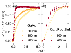 The dynamic increase in THz photoconductivity resulting from energetic intraband relaxation was used to track the formation of highly mobile charges in thin films of the tin iodide perovskite Cs1-xRbxSnI3, with x=0 and x=0.1. Energy relaxation times were found to be around 500fs, comparable to those in the prototypical inorganic semiconductor GaAs. At low excess energies the efficient intraband energy relaxation in the lowest conduction and valence bands of Cs1-xRbxSnI3 can be understood within the context of the Fröhlich electron-phonon interaction, with a strong coupling strength. For higher excess energies the photoconductivity rise time lengthens in accordance with carrier injection into multiple bands, identified by quantitative first-principles bandstructure calculations and photoluminescence spectroscopy. The findings contribute to the development of design rules for photovoltaic devices capable of extracting hot carriers from perovskite semiconductors.