Ultrafast & Terahertz Photonics Group
|
Ultrafast optical techniques provide powerful probes of different states of matter, using light pulses that have femtosecond duration. In Warwick our activities span a number of areas:
|
Group facilitiesThe Group has labs across the campus, in the main Physics building, Materials and Analytical Sciences, and Millburn House. Read more about our experimental capabilities in terahertz science and technology. We also run the Warwick Centre for Ultrafast Spectroscopy Research Technology Platform. 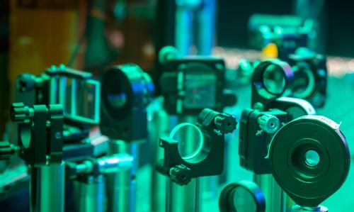
We make use of a wide range of Warwick's excellent materials analysis equipment, including X-ray diffraction, Raman spectroscopy, electron microscopy and magnetometry. |
Join the group!Please get in touch if you are interested in a PhD or MSc by Research in the group. We are also happy to support postdoctoral researchers to apply for fellowship schemes. 
Group, Theses & PhotosContact details for our current group members and our photo gallery. For recent theses from the group, please see here. |
Research areas
Nanomaterials
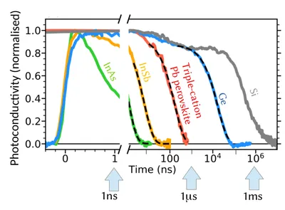
We use pump/probe spectroscopy to study how light and matter interact on femtosecond to nanosecond timescales. Using visible probes we can track electronic processes, while infrared radiation lets us study vibrational states of molecules and atomic-scale defects in semiconductors.
Recent papers:
Quantifying photoluminescence variability in monolayer molybdenum disulfide films grown by chemical vapour deposition
The 3237 cm−1 diamond defect: Ultrafast vibrational dynamics, concentration calibration, and relationship to the N3VH0 defect
Terahertz medical imaging
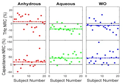
Performing in vivo studies of the THz properties of skin is a major initiative in the group, supported by the EPSRC Terabotics Programme GrantLink opens in a new window. We develop robust measurement protocols and test them on a statistically significant number of patients, cross-checking with other methods.
Recent papers:
Terahertz probe for real time in vivo skin hydration evaluation
Spectroscopic insight on impact of environment on natural photoprotectants
The 2023 terahertz science and technology roadmap
Semiconductors and Energy materials
A major strand of our research is to improve our knowledge of the fundamental science underpinning new semiconductor materials, such as metal-halide perovskites, which are often attractive for photovoltaic applications.
Recent papers:
Distinguishing carrier transport and interfacial recombination at perovskite/transport-layer interfaces using ultrafast spectroscopy and numerical simulation
Temperature-Dependent Structural and Optoelectronic Properties of the Layered Perovskite 2-Thiophenemethylammonium Lead Iodide
Terahertz Emission via Optical Rectification in a Metal-Free Perovskite Crystal
Terahertz components, methods and techniques
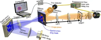
We develop new THz devices and integrate them into novel systems designs that can perform THz imaging and THz spectroscopy faster, and with increased capabilities (e.g. polarisation control; robot-controlled probes).
Recent papers:
Simultaneous measurement of orthogonal terahertz fields via an emission multiplexing scheme
Optimum Optical Designs for Diffraction-Limited Terahertz Spectroscopy and Imaging Systems Using Off-Axis Parabolic Mirrors
The 2023 terahertz science and technology roadmap
Recent publication highlights [filter by topic: view all | highlights | THz | perovskites | nano | biomedical]
Efficient Intraband Hot Carrier Relaxation in the Perovskite Semiconductor Cs1-xRbxSnI3 Mediated by Strong Electron-Phonon Coupling
M. Monti, S. Tao, M. Staniforth, A. Crocker, E. Griffin, A. Wijesekara, R.A. Hatton, and J. Lloyd-Hughes
J. Phys. Chem. C 122 20669 (Aug 2018) [ pdf ] [ ref ]
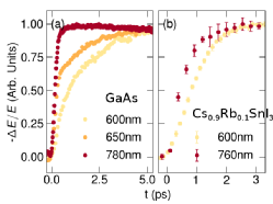 The dynamic increase in THz photoconductivity resulting from energetic intraband relaxation was used to track the formation of highly mobile charges in thin films of the tin iodide perovskite Cs1-xRbxSnI3, with x=0 and x=0.1. Energy relaxation times were found to be around 500fs, comparable to those in the prototypical inorganic semiconductor GaAs. At low excess energies the efficient intraband energy relaxation in the lowest conduction and valence bands of Cs1-xRbxSnI3 can be understood within the context of the Fröhlich electron-phonon interaction, with a strong coupling strength. For higher excess energies the photoconductivity rise time lengthens in accordance with carrier injection into multiple bands, identified by quantitative first-principles bandstructure calculations and photoluminescence spectroscopy. The findings contribute to the development of design rules for photovoltaic devices capable of extracting hot carriers from perovskite semiconductors.
Highly Sensitive Terahertz Thin-Film Total Internal Reflection Spectroscopy Reveals in Situ Photoinduced Structural Changes in Methylammonium Lead Halide Perovskites
Q. Sun, X. Liu, J. Cao, R.I. Stantchev, Y. Zhou, X. Chen, E.P.J. Parrott, J. Lloyd-Hughes, N. Zhao, and E. Pickwell-MacPherson
J. Phys. Chem. C 122 17552 (June 2018) [ pdf ] [ ref ]
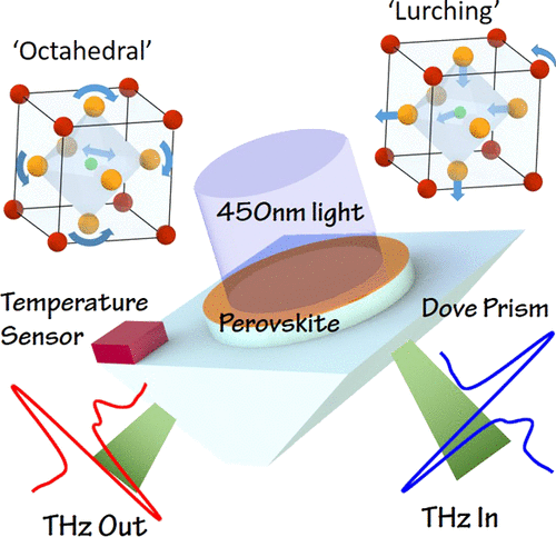
Terahertz (THz) thin-film total internal reflection (TF-TIR) spectroscopy is shown to have an enhanced sensitivity to the vibrational properties of thin films in comparison with standard THz transmission spectroscopy. This increased sensitivity was used to track photoinduced modifications to the structure of thin films of methylammonium (MA) lead halide, MAPbI3–xBrx (x = 0, 0.5, 1, and 3). Initially, illumination strengthened the phonon modes around 2 THz, associated with Pb–I stretch modes coupled to the MA ions, whereas the 1 THz twist modes of the inorganic octahedra did not alter in strength. Under longer term illumination, the 1 THz phonon modes of encapsulated films slowly reduced in strength, whereas in films exposed to moisture and oxygen, these phonons weaken more rapidly and blue-shift in frequency. The rapid monitoring of environmentally induced changes to the vibrational modes afforded by TF-TIR spectroscopy offers applications in the characterization and quality control of the perovskite thin-film solar cells and other thin-film semiconductors.
Cs1−xRbxSnI3 light harvesting semiconductors for perovskite photovoltaics
K.P. Marshall, S. Tao, M. Walker, D.S. Cook, J. Lloyd-Hughes, S. Varagnolo, A. Wijesekara, D. Walker, R.I. Walton and R.A. Hatton
Materials Chemistry Frontiers 2:1515 (June 2018) [ pdf ] [ ref ]
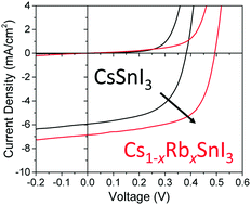
We show that films of the 3-dimensional perovskite Cs1−xRbxSnI3 can be prepared from room temperature N,N-dimethylformamide solutions of RbI, CsI and SnCl2 for x ≤ 0.5, and that for x ≤ 0.2 film stability is sufficient for utility as the light harvesting layer in inverted photovoltaic (PV) devices. Electronic absorption and photoluminescence spectroscopy measurements supported by computational simulation, show that increasing x increases the band gap, due to distortion of the lattice of SnI6 octahedra that occurs when Cs is substituted with Rb, although it also reduces the stability towards decomposition. When Cs0.8Rb0.2SnI3 perovskite is incorporated into the model inverted PV device structure; ITO|perovskite|C60|bathocuproine|Al, an ∼120 mV increase in open-circuit is achieved which is shown to correlate with an increase in perovskite ionisation potential. However, for this low Rb loading the increase in band gap is very small (∼30 meV) and so a significant increase in open circuit-voltage is achieved without reducing the range of wavelengths over which the perovskite can harvest light. The experimental findings presented are shown to agree well with the predictions of density functional theory (DFT) simulations of the stability and electronic structure, also performed as part of this study.
Conduction properties of thin films from a water soluble carbon nanotube/hemicellulose complex
D. Shao, P. Yotprayoonsak, V. Saunajoki, M. Ahlskog, J. Virtanen, V. Kangas, A. Volodin, C. Van Haesendonck, M. Burdanova, C. D. W. Mosley and J. Lloyd-Hughes
Nanotechnology 29 145203 (Feb 2018) [ pdf ] [ ref ]
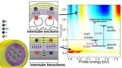
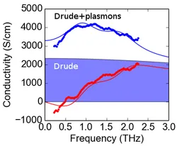 We have examined the conductive properties of a carbon nanotube (CNT) based thin film, which were prepared via dispersion in water by non-covalent functionalization of the nanotubes with xylan, a type of hemicellulose. Measurements of low temperature conductivity, Kelvin Probe Force Microscopy, and high frequency (THz) conductivity elucidated the intra-tube and inter-tube charge transport processes in this material. The measurements show excellent conductive properties of the as prepared thin films, with bulk conductivity up to 2000 S/cm. The transport results demonstrate that the hemicellulose does not seriously interfere with the inter-tube conductance.